LTC1069-1IS8#PBF

LTC1069-1
7
10691fa
APPLICATIONS INFORMATION
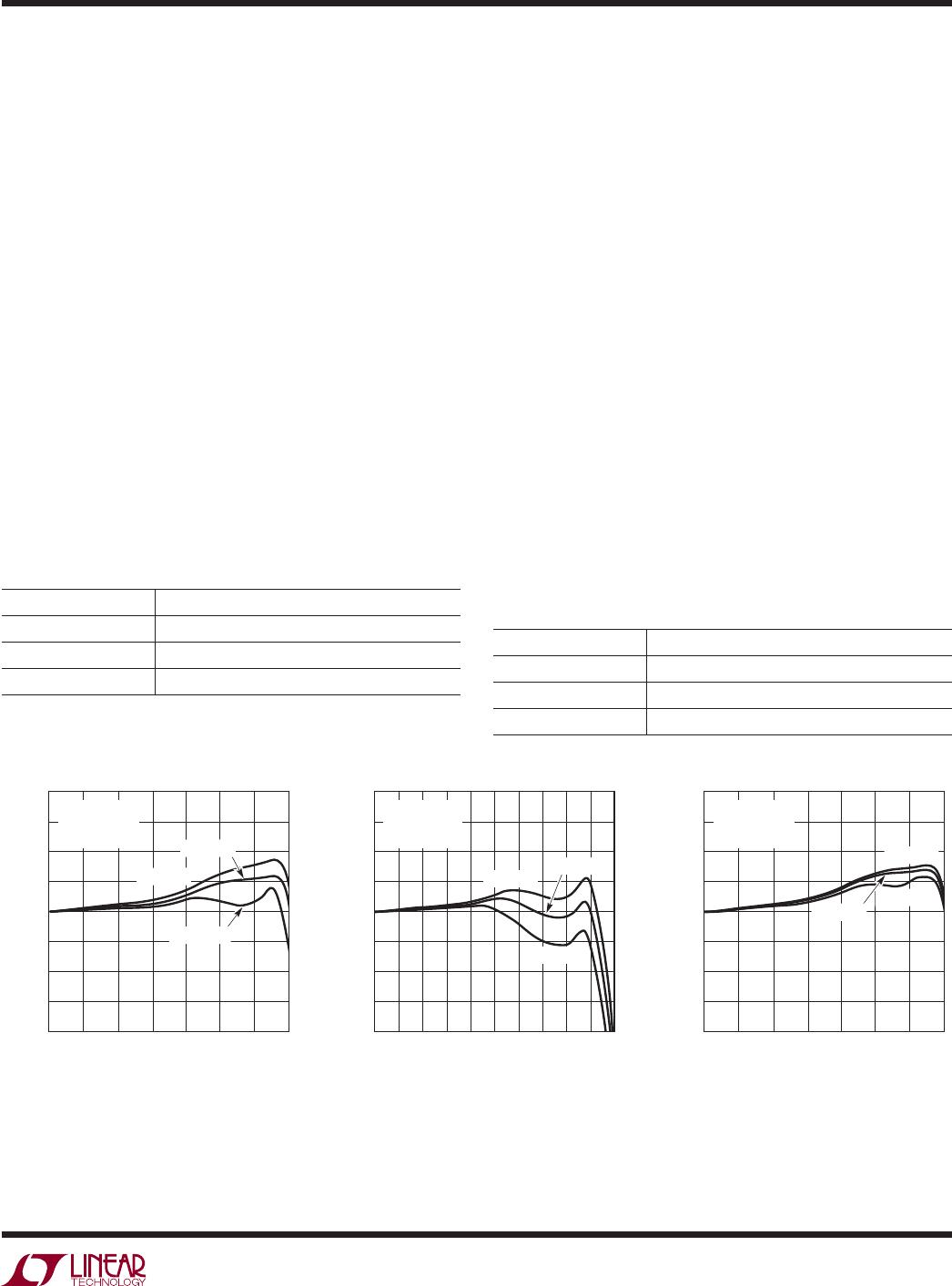
Temperature Behavior
The power supply current of the LTC1069-1 has a positive
temperature coeffi cient. The GBW product of its internal
op amps is nearly constant and the speed of the device
does not degrade at high temperatures. Figures 3a, 3b and
3c show the behavior of the maximum passband of the
device for various supplies and temperatures. The fi lter,
especially at ±5V supply, has a passband behavior which
is nearly temperature independent.
Clock Feedthrough
The clock feedthrough is defi ned as the RMS value of the
clock frequency and its harmonics that are present at the
lters output pin (8). The clock feedthrough is tested with
the input pin (4) shorted to the AGND pin and depends on
PC board layout and on the value of the power supplies.
With proper layout techniques the values of the clock
feedthrough are shown on Table 2.
Table 2. Clock Feedthrough
V
S
CLOCK FEEDTHROUGH
3.3V 10μV
RMS
5V 40μV
RMS
±5V 160μVRMS
Any parasitic switching transients during the rise and
fall edges of the incoming clock are not part of the clock
feedthrough specifi cations. Switching transients have
frequency contents much higher than the applied clock;
their amplitude strongly depends on scope probing tech-
niques as well as grounding and power supply bypassing.
The clock feedthrough can be reduced, if bothersome, by
adding a single RC lowpass fi lter at the output pin (8) of
the LTC1069-1.
Wideband Noise
The wideband noise of the fi lter is the total RMS value
of the device’s noise spectral density and determines the
operating signal-to-noise ratio. Most of the wideband
noise frequency contents lie within the fi lter passband.
The wideband noise cannot be reduced by adding post
ltering. The total wideband noise is nearly independent
of the clock frequency and depends slightly on the power
supply voltage (see Table 3). The clock feedthrough speci
cations are not part of the wideband noise.
Table 3. Wideband Noise
V
S
WIDEBAND NOISE
3.3V 100μV
RMS
5V 108μV
RMS
±5V 112μV
RMS
Figure 3a Figure 3b Figure 3c
FREQUENCY (kHz)
0.5
GAIN (dB)
6.5
10691 F03a
2.5 4.5
2.0
1.5
1.0
0.5
0
–0.5
–1.0
–1.5
–2.0
1.5 3.5 5.5 7.5
V
S
= 3.3V
f
CLK
= 750kHz
V
IN
= 0.5V
RMS
T
A
= 85°C
T
A
= 25°C
T
A
= –40°C
FREQUENCY (kHz)
0.5
GAIN (dB)
6.5
10691 F03b
2.5 4.5
2.0
1.5
1.0
0.5
0
–0.5
–1.0
–1.5
–2.0
1.5 3.5 5.5 7.5 8.5 9.5 10.5
V
S
= 5V
f
CLK
= 1MHz
V
IN
= 1.2V
RMS
T
A
= 25°C
T
A
= 85°C
T
A
= –40°C
FREQUENCY (kHz)
1
GAIN (dB)
13
10691 F03c
59
2.0
1.5
1.0
0.5
0
–0.5
–1.0
–1.5
–2.0
3 7 11 15
V
S
= ±5V
f
CLK
= 1.5MHz
V
IN
= 2V
RMS
T
A
= 85°C
T
A
= –40°C
T
A
= 25°C
LTC1069-1
8
10691fa
APPLICATIONS INFORMATION
Aliasing
Aliasing is an inherent phenomenon of sampled data
systems and it occurs for input frequencies approaching
the sampling frequency. The internal sampling frequency
of the LTC1069-1 is 100 times its cutoff frequency. For
instance, if a 98kHz, 100mV
RMS
signal is applied at the
input of an LTC1069-1 operating with a 100kHz clock, a
2kHz, 28μV
RMS
alias signal will appear at the fi lter output.
Table 4 shows details.
Table 4. Aliasing (f
CLK
= 100kHz)
INPUT FREQUENCY
(V
IN
= 1V
RMS
)
(kHz)
OUTPUT LEVEL
(Relative to Input)
(dB)
OUTPUT FREQUENCY
(Aliased Frequency)
(kHz)
f
CLK
/f
C
= 100:1, f
CUTOFF
= 1kHz
96 (or 104)
97 (or 103)
98 (or 102)
98.5 (or 101.5)
99 (or 101)
99.5 (or 100.5)
–90.0
–86.0
–71.0
–56.0
–1.1
–0.21
4.0
3.0
2.0
1.5
1.0
0.5
TYPICAL APPLICATIONS
Single 3.3V Supply Operation with Output Buffer
Single 5V Operation with Power Shutdown
1
2
3
4
8
7
6
5
V
OUT
V
NC
CLK
AGND
V
+
NC
V
IN
0.1μF
0.47μF
SHUTDOWN
ON
5V
V
IN
V
OUT
1069-1 TA04
LTC1069-1
f
CLK
750kHz
5V
0V
CMOS LOGIC
1
2
3
4
8
7
6
5
V
OUT
V
NC
CLK
AGND
V
+
NC
V
IN
0.1μF
0.47μF
V
IN
V
OUT
10691 TA05
LTC1069-1
f
CLK
500kHz
3.3V
0V
+
1/2 LT1366
3.3V
0.1μF
LTC1069-1
9
10691fa
Information furnished by Linear Technology Corporation is believed to be accurate and reliable.
However, no responsibility is assumed for its use. Linear Technology Corporation makes no representa-
tion that the interconnection of its circuits as described herein will not infringe on existing patent rights.
.016 – .050
(0.406 – 1.270)
.010 – .020
(0.254 – 0.508)
× 45°
0°– 8° TYP
.008 – .010
(0.203 – 0.254)
SO8 0303
.053 – .069
(1.346 – 1.752)
.014 – .019
(0.355 – 0.483)
TYP
.004 – .010
(0.101 – 0.254)
.050
(1.270)
BSC
1
2
3
4
.150 – .157
(3.810 – 3.988)
NOTE 3
8
7
6
5
.189 – .197
(4.801 – 5.004)
NOTE 3
.228 – .244
(5.791 – 6.197)
.245
MIN
.160
±.005
RECOMMENDED SOLDER PAD LAYOUT
.045 ±.005
.050 BSC
.030 ±.005
TYP
INCHES
(MILLIMETERS)
NOTE:
1. DIMENSIONS IN
2. DRAWING NOT TO SCALE
3. THESE DIMENSIONS DO NOT INCLUDE MOLD FLASH OR PROTRUSIONS.
MOLD FLASH OR PROTRUSIONS SHALL NOT EXCEED .006" (0.15mm)
N8 1002
.065
(1.651)
TYP
.045 – .065
(1.143 – 1.651)
.130 ± .005
(3.302 ± 0.127)
.020
(0.508)
MIN
.018 ± .003
(0.457 ± 0.076)
.120
(3.048)
MIN
12
3
4
87 6
5
.255 ± .015*
(6.477 ± 0.381)
.400*
(10.160)
MAX
.008 – .015
(0.203 – 0.381)
.300 – .325
(7.620 – 8.255)
.325
+.035
–.015
+0.889
0.381
8.255
()
NOTE:
1. DIMENSIONS ARE
INCHES
MILLIMETERS
*THESE DIMENSIONS DO NOT INCLUDE MOLD FLASH OR PROTRUSIONS.
MOLD FLASH OR PROTRUSIONS SHALL NOT EXCEED .010 INCH (0.254mm)
.100
(2.54)
BSC
PACKAGE DESCRIPTION
S8 Package
8-Lead Plastic Small Outline (Narrow .150 Inch)
(Reference LTC DWG # 05-08-1610)
N Package
8-Lead PDIP (Narrow .300 Inch)
(Reference LTC DWG # 05-08-1510)

LTC1069-1IS8#PBF

Mfr. #:
Manufacturer:
Analog Devices Inc.
Description:
Active Filter L/P 8th Order Progress Elliptic LPF
Lifecycle:
New from this manufacturer.
Delivery:
DHL FedEx Ups TNT EMS
Payment:
T/T Paypal Visa MoneyGram Western Union