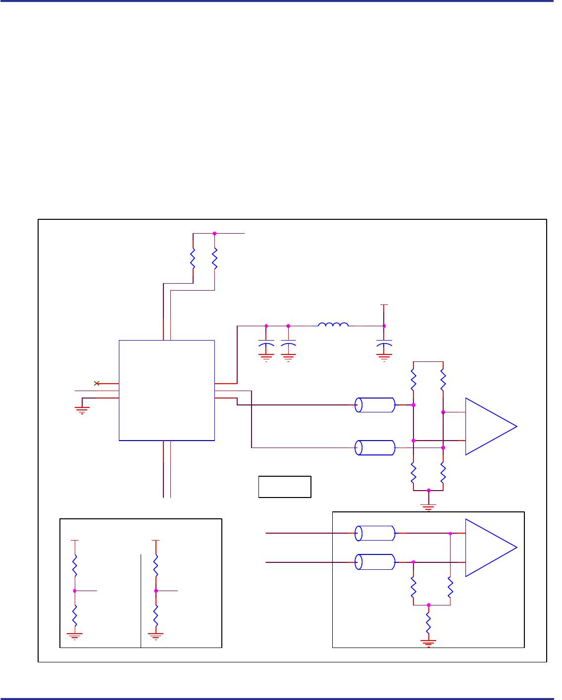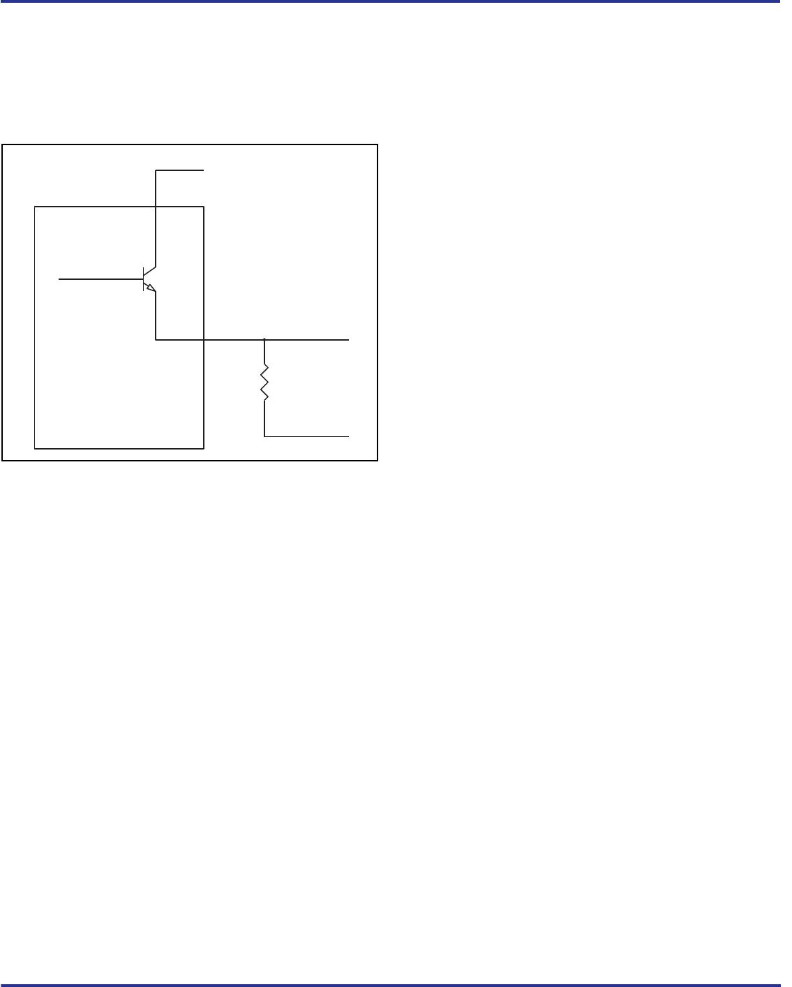
IDT8N3Q001 REV G Data Sheet QUAD-FREQUENCY PROGRAMMABLE-XO
IDT8N3Q001GCD REVISION A
MARCH 6, 2012
14 ©2012 Integrated Device Technology, Inc.
Power Considerations
This section provides information on power dissipation and junction temperature for the IDT8N3Q001.
Equations and example calculations are also provided.
1. Power Dissipation.
The total power dissipation for the IDT8N3Q001 is the sum of the core power plus the power dissipated in the load(s).
The following is the power dissipation for V
CC
= 3.465V, which gives worst case results.
NOTE: Please refer to Section 3 for details on calculating power dissipated in the load.
• Power (core)
MAX
= V
CC_MAX
* I
EE_MAX
= 3.465V * 140mA = 485.1mW
• Power (outputs)
MAX
= 34.2mW/Loaded Output pair
Total Power_
MAX
(3.465V, with all outputs switching) = 485.1mW + 34.2mW = 519.3mW
2. Junction Temperature.
Junction temperature, Tj, is the temperature at the junction of the bond wire and bond pad directly affects the reliability of the device. The
maximum recommended junction temperature is 125°C. Limiting the internal transistor junction temperature, Tj, to 125°C ensures that the bond
wire and bond pad temperature remains below 125°C.
The equation for Tj is as follows: Tj =
JA
* Pd_total + T
A
Tj = Junction Temperature
JA
= Junction-to-Ambient Thermal Resistance
Pd_total = Total Device Power Dissipation (example calculation is in section 1 above)
T
A
= Ambient Temperature
In order to calculate junction temperature, the appropriate junction-to-ambient thermal resistance
JA
must be used. Assuming no air flow and
a multi-layer board, the appropriate value is 49.4°C/W per Table 7 below.
Therefore, Tj for an ambient temperature of 85°C with all outputs switching is:
85°C + 0.519W * 49.4°C/W = 110.7°C. This is below the limit of 125°C.
This calculation is only an example. Tj will obviously vary depending on the number of loaded outputs, supply voltage, air flow and the type of
board (multi-layer).
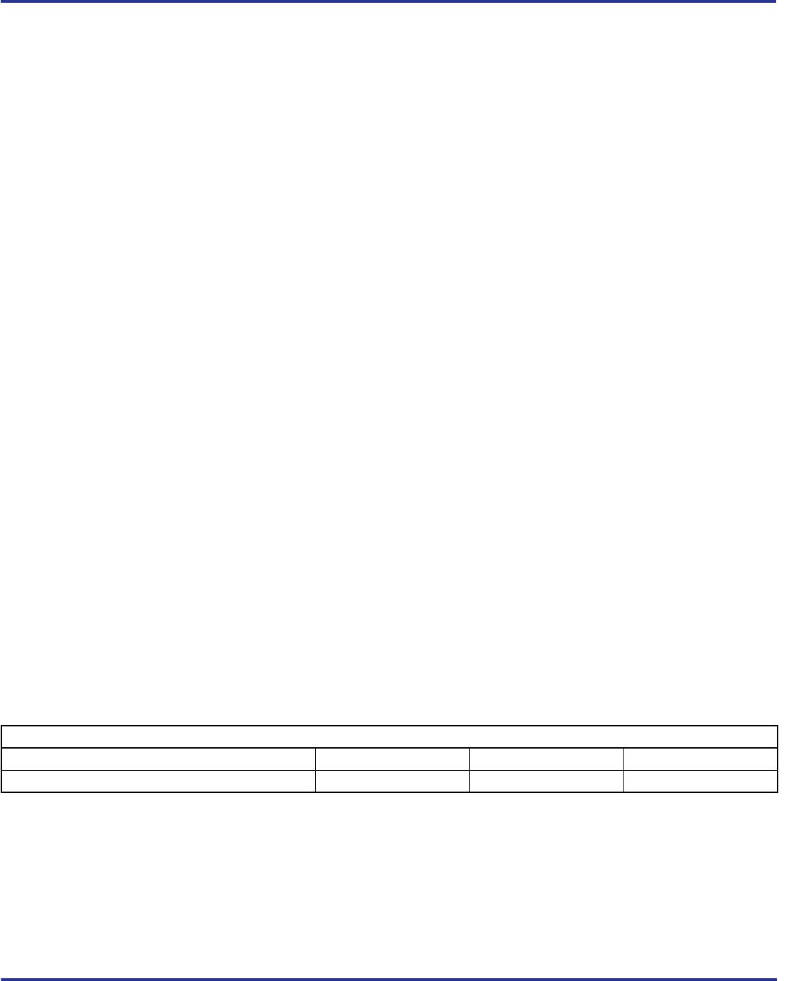
Table 7. Thermal Resistance
JA
for 10 Lead Ceramic 5mm x 7mm Package, Forced Convection
JA
by Velocity
Meters per Second 012.5
Multi-Layer PCB, JEDEC Standard Test Boards 49.4°C/W 44.2°C/W 41°C/W