IDT8N3Q001 REV G Data Sheet QUAD-FREQUENCY PROGRAMMABLE-XO
IDT8N3Q001GCD REVISION A
MARCH 6, 2012
7 ©2012 Integrated Device Technology, Inc.
NOTE: Electrical parameters are guaranteed over the specified ambient operating temperature range, which is established when the device
is mounted in a test socket with maintained transverse airflow greater than 500 lfpm. The device will meet specifications after thermal
equilibrium has been reached under these conditions.
NOTE: XTAL parameters (initial accuracy, temperature stability, aging and total stability) are guaranteed by manufacturing.
NOTE 1: This parameter is defined in accordance with JEDEC standard 65.
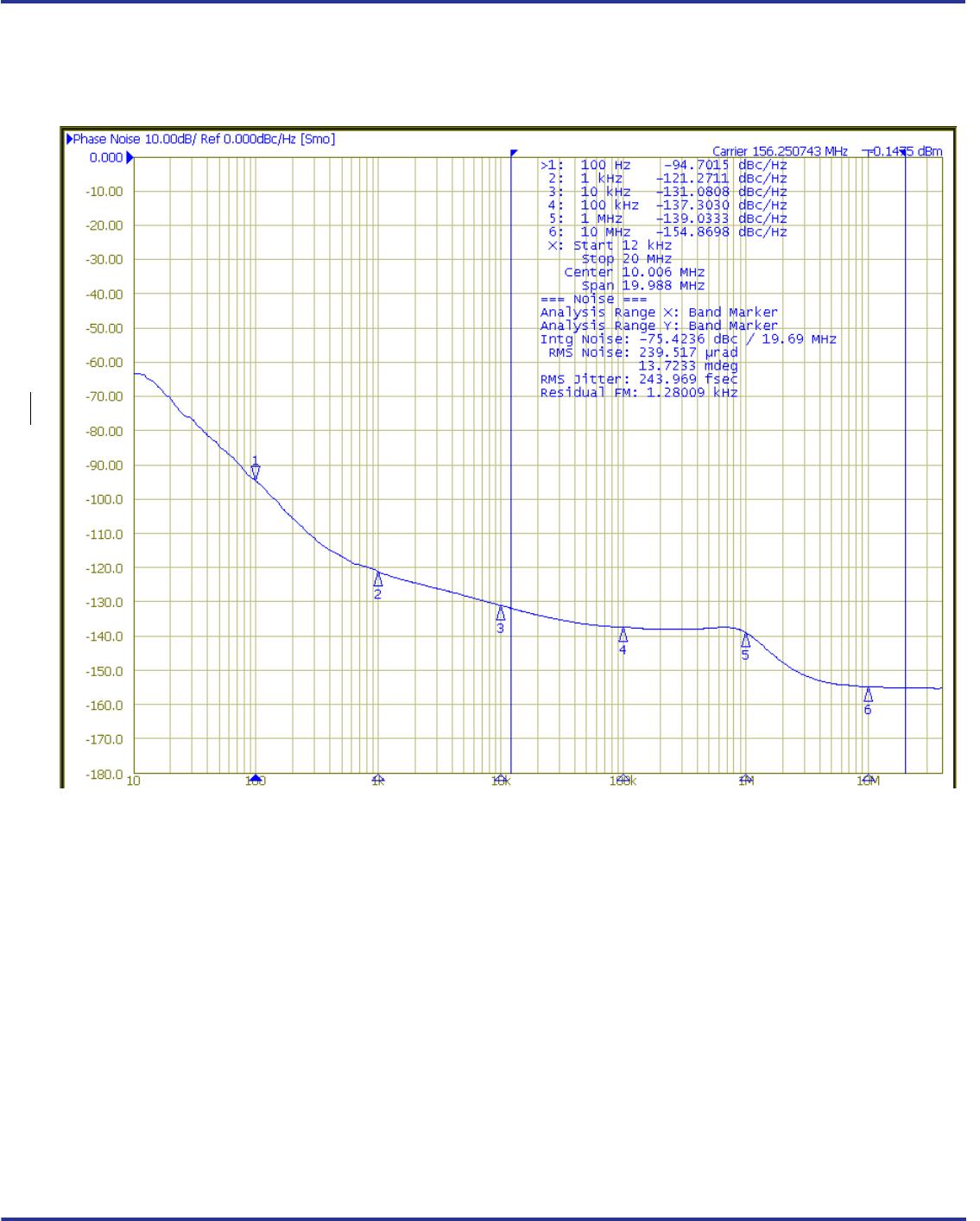
NOTE 2: Please refer to the phase noise plots.
NOTE 3: Please see the FemtoClockNG Ceramic 5x7 Modules Programming guide for more information on PLL feedback modes and the
optimum configuration for phase noise. Integer PLL feedback is the default operation for the dddd = 1xxx order codes and configures
DSM_ENA = 0 and ADC_EN = 0.
NOTE 4: Integration range: 12kHz-20MHz.
NOTE 5: Integration range: 1kHz-40MHz.
N
(100k)
Single-side band phase noise,
100kHz from Carrier
156.25MHz -137.3 dBc/Hz
N
(1M)
Single-side band phase noise,
1MHz from Carrier
156.25MHz -139.0 dBc/Hz
N
(10M)
Single-side band phase noise,
10MHz from Carrier
156.25MHz -154.9 dBc/Hz
PSNR Power Supply Noise Rejection
50mV Sinusoidal Noise
1kHz - 50kHz
-54 dB
t
R
/ t
F
Output Rise/Fall Time 20% to 80% 100 425 ps
odc Output Duty Cycle 45 55 %
t
STARTUP
Oscillator Start-Up Time 20 ms
t
SET
Output frequency settling time after
FSEL0 and FSEL1 values are changed
470 µs
Symbol Parameter Test Conditions Minimum Typical Maximum Units