August 2006 Rev 7 1/14
14
STB24NF10
STP24NF10
N-channel 100V - 0.0055 - 26A - TO-220 - D²PAK
Low gate charge STripFET™ II Power MOSFET
General features
Exceptional dv/dt capability
100% avalanche tested
Application oriented characterization
Description
This Power MOSFET series realized with
STMicroelectronics unique STripFET™ process
has specifically been designed to minimize the
on-resistance. It is therefore suitable as primary
switch in advanced high-efficiency,high-frequency
isolated DC-DC converters for Telecom and
Computer application. It is also intended for any
applications with low gate drive requirements.
Applications
Switching application
Internal schematic diagram
Type V
DSS
R
DS(on)
I
D
STB24NF10
STP24NF10
100V
100V
<0.060
<0.060
26A
26A
1
3
1
2
3
TO-220
D²PAK
www.st.com
Order codes
Part number Marking Package Packaging
STP24NF10 P24NF10 TO-220 Tube
STB24NF10 B24NF10 D²PAK Tape & reel
Contents STB24NF10 - STP24NF10
2/14
Contents
1 Electrical ratings . . . . . . . . . . . . . . . . . . . . . . . . . . . . . . . . . . . . . . . . . . . . 3
2 Electrical characteristics . . . . . . . . . . . . . . . . . . . . . . . . . . . . . . . . . . . . . 4
2.1 Electrical characteristics (curves) . . . . . . . . . . . . . . . . . . . . . . . . . . . . 6
3 Test circuit . . . . . . . . . . . . . . . . . . . . . . . . . . . . . . . . . . . . . . . . . . . . . . . . 8
4 Package mechanical data . . . . . . . . . . . . . . . . . . . . . . . . . . . . . . . . . . . . . 9
5 Packaging mechanical data . . . . . . . . . . . . . . . . . . . . . . . . . . . . . . . . . . 12
6 Revision history . . . . . . . . . . . . . . . . . . . . . . . . . . . . . . . . . . . . . . . . . . . 13
STB24NF10 - STP24NF10 Electrical ratings
3/14
1 Electrical ratings
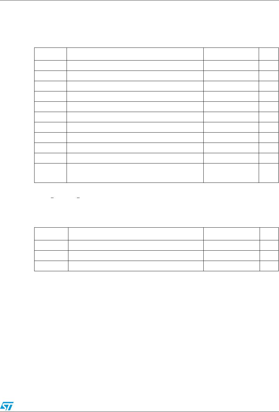
Table 1. Absolute maximum ratings
Symbol Parameter Value Unit
V
DS
Drain-source voltage (V
GS
= 0) 100 V
V
DGR
Drai-gate voltage (R
GS
=20k) 100 V
V
GS
Gate-source voltage ± 20 V
I
D
Drain current (continuous) at T
C
= 25°C 26 A
I
D
Drain current (continuous) at T
C
=100°C 18 A
I
DM
(1)
1. Pulse width limited by safe operating area.
Drain current (pulsed) 104 A
P
TOT
Total dissipation at T
C
= 25°C 85 W
Derating factor 0.57 W/°C
dv/dt
(2)
2. I
SD
< 24A, di/dt < 300A/µs, V
DD
=80%V
(BR)DSS
Peak diode recovery voltage slope 9 V/ns
E
AS
(3)
3. Starting Tj = 25°C, I
D
=12A, V
DD
=30V
Single pulse avalanche energy 220 mJ
T
J
T
stg
Operating junction temperature
Storage temperature
-55 to 175 °C
Table 2. Thermal resistance
Symbol Parameter Value Unit
R
thj-case
Thermal resistance junction-case Max 1.76 °C/W
R
thj-amb
Thermal resistance junction-ambient Max 62.5 °C/W
T
j
Maximum lead temperature for soldering purpose 300 °C

STP24NF10

Mfr. #:
Manufacturer:
STMicroelectronics
Description:
MOSFET N-Ch 100 Volt 24 Amp
Lifecycle:
New from this manufacturer.
Delivery:
DHL FedEx Ups TNT EMS
Payment:
T/T Paypal Visa MoneyGram Western Union

Products related to this Datasheet