1
ZXSC300
ISSUE 4 - SEPTEMBER 2007
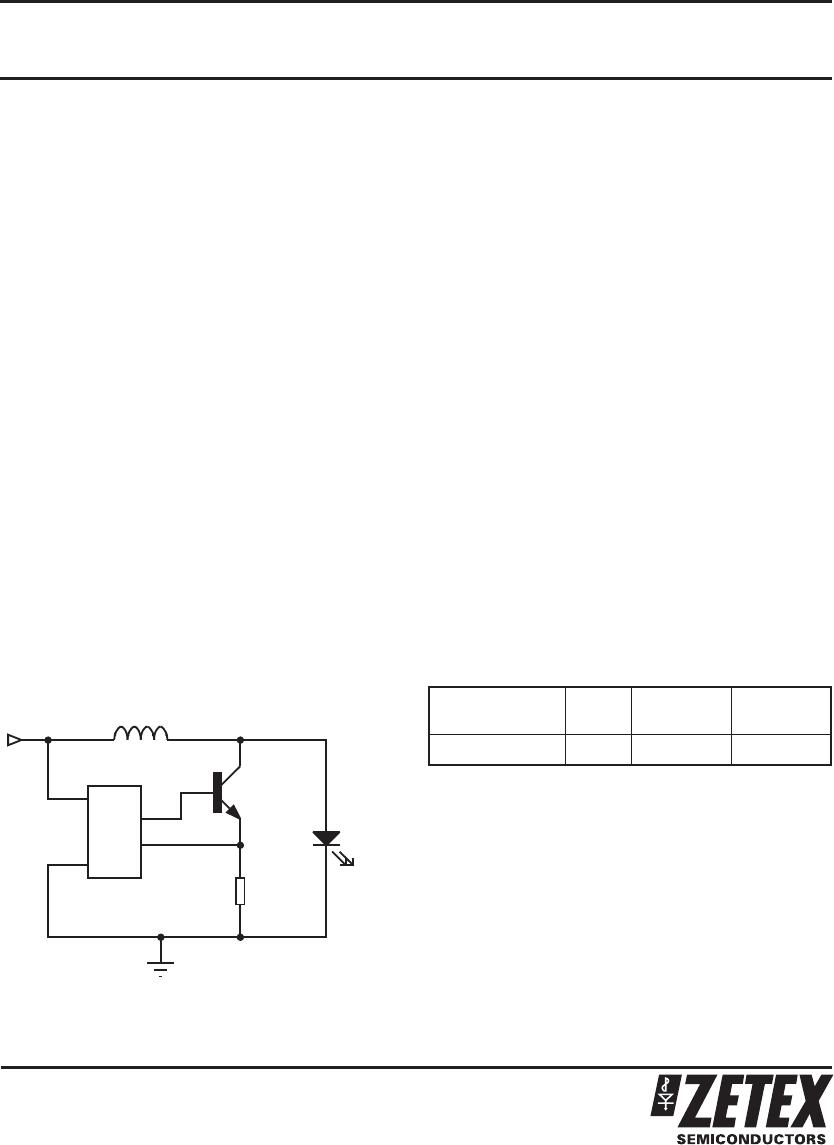
SINGLE OR MULTI CELL LED DRIVER SOLUTION
Q1
FMMT617
R1
0.33R
L1
100µH
V
BATT
LED1
WHITE LED
V
cc
Gnd
I
sense
V
drive
U1
ZXSC300
TYPICAL APPLICATION CIRCUIT
ORDERING INFORMATION
DEVICE Reel Tapewidth Quantity
per reel
ZXSC300E5TA 7” 8mm 3,000
DEVICE MARKING C300
Package SOT23-5
DESCRIPTION
The ZXSC300 is a single or multi cell LED driver
designed for applications where step-up voltage
conversion from very low input voltages is required.
These applications mainly operate from single 1.5V or
1.2V battery cells. The circuit generates constant
current pulses that are ideal for driving single or
multiple LED’s over a wide range of operating voltages.
The ZXSC300 is a PFM controller IC that drives an
external Zetex switching transistor with a very low
saturation resistance. These transistors are the best
switching devices available for this type of switching
conversion enabling high efficiency conversion with
input voltages below 1 volt. The drive output of the
ZXSC controller generates a dynamic drive signal for
the switching transistor.
FEATURES
94% efficiency
Minimum operating input voltage 0.8V
Fixed output current
Low saturation voltage switching transistor
SOT23-5 package
The circuit can start up under full load and operates
down to an input voltage of 0.8 volts. The solution
configuration ensures optimum efficiency over a wide
range of load currents, several circuit configurations
are possible depending on battery life versus
brightness considerations.
The ZXSC300 is offered in the SOT23-5 package which,
when combined with a SOT23 switching transistor,
generates a high efficiency small size circuit solution.
The IC and discrete combination offers the ultimate
cost vs performance solution for single cell LED driving
applications.
APPLICATIONS
LED flashlights and torches
LED backlights
White LED driving
Multiple LED driving
Solar Equipment
ABSOLUTE MAXIMUM RATING
ZXSC300
ISSUE 4 - SEPTEMBER 2007
2
Supply Voltage -0.3 to 10V
Maximum Voltage Other Pins -0.3 to V
CC
+0.3V
Power Dissipation 450mW
Operating Temperature -40 to 85°C
Storage Temperature -55 to 150°C
ELECTRICAL CHARACTERISTICS: Test conditions unless otherwise stated: V
CC
=1.5V, T
AMB
=25°C
SYMBOL PARAMETER CONDITIONS MIN. TYP. MAX. UNITS
η
Efficiency
(1)
94 %
V
CC
Recommended
supply voltage range
0.8 8 V
V
CC(min)
Minimum startup
and operating
voltage
I
DRIVE
=-600µA, V
DRIVE
=0.7V
I
DRIVE
=-600µA, V
DRIVE
=0.7V,
T
AMB
=-10°C
(3)
0.8
0.9
0.92 V
I
Q
Quiescent current
(2)
0.2 mA
I
VDRIVE
Base drive current V
DRIVE
=0.7V,V
ISENSE
=0V 1.5 3.6 mA
I
CC
Supply current
(3)
V
DRIVE
=0.7V,V
ISENSE
=0V 2 4 mA
V
VDRIVE(high)
High level drive
voltage
V
ISENSE
=0V,I
VDRIVE
=-0.5mA V
CC
-0.3 V
CC
V
V
VDRIVE(low)
Low level drive
voltage
V
ISENSE
=50mV,I
VDRIVE
=5mA 0 0.2 V
V
ISENSE
(threshold)
Output current
reference voltage
14 19 24 mV
T
CVISENSE
I
SENSE
voltage temp co.
2
0.4 %/°C
I
ISENSE
I
SENSE
input current V
ISENSE
=0V 0 -30 -65 µA
T
DRV
Discharge pulse width 1.2 1.7 3.2 µs
SYMBOL PARAMETER CONDITIONS MIN. TYP. MAX. UNITS
F
OSC
Recommended operating frequency
(4)
200 kHz
1
Application dependent, see reference designs.
2
These parameters guaranteed by design and characterisation
3
Total supply current =I
Q
+ I
VDRIVE
, see typical characteristics
4
Operating frequency is application circuit dependent. See applications section.
OPERATING CONDITIONS
ZXSC300
ISSUE 4 - SEPTEMBER 2007
3
FMMT617
For the circuits described in the applications section, Zetex FMMT617 is the recommended pass transistor. The
following indicates outline data for the transistor, more detailed information can be found at
www.zetex.com/FMMT617
ELECTRICAL CHARACTERISTICS (at T
A
= 25°C unless otherwise stated).
PARAMETER SYMBOL MIN. TYP. MAX. UNIT CONDITIONS
Collector-Emitter
Saturation Voltage
V
CE(sat)
8
70
150
14
100
200
mV
mV
mV
I
C
=0.1A, I
B
=10mA*
I
C
=1A, I
B
=10mA*
I
C
=3A, I
B
=40mA*
Collector-Emitter
Breakdown Voltage
V
(BR)CEO
15 18 V I
C
=10mA*
*Measured under pulsed conditions. Pulse width=300μs. Duty cycle 2%
ZHCS1000
For the circuits described in the applications section Zetex ZHCS1000 is the recommended Schottky diode. The
following indicates outline data for the diode, more detailed information is available at www.zetex.com
ELECTRICAL CHARACTERISTICS (at T
amb
= 25°C unless otherwise stated).
PARAMETER SYMBOL MIN. TYP. MAX. UNIT CONDITIONS
Forward Voltage V
F
400
500
mV
mV
I
F
=500mA
I
F
=1A
Reverse Current I
R
50 100
μA
V
R
=30V
Reverse Recovery
Time
t
rr
12 ns Switched from I
F
= 500mA
to I
R
= 500mA. Measured
at I
R
=50mA
*Measured under pulsed conditions. Pulse width=300μs. Duty cycle 2%

ZXSC300E5TA

Mfr. #:
Manufacturer:
Diodes Incorporated
Description:
LED Lighting Drivers Sgl/Multi Cl LED Dvr
Lifecycle:
New from this manufacturer.
Delivery:
DHL FedEx Ups TNT EMS
Payment:
T/T Paypal Visa MoneyGram Western Union

Products related to this Datasheet