RT9010-12GJ6

RT9010
4
DS9010-05 April 2011www.richtek.com
Note 1. Stresses listed as the above "Absolute Maximum Ratings" may cause permanent damage to the device. These are for
stress ratings. Functional operation of the device at these or any other conditions beyond those indicated in the
operational sections of the specifications is not implied. Exposure to absolute maximum rating conditions for extended
periods may remain possibility to affect device reliability.
Note 2. θ
JA
is measured in the natural convection at T
A
= 25°C on a low effective thermal conductivity test board of
JEDEC 51-3 thermal measurement standard.
Note 3. Devices are ESD sensitive. Handling precaution recommended.
Note 4. The device is not guaranteed to function outside its operating conditions.
Note 5. The dropout voltage is defined as V
IN
-V
OUT
, which is measured when V
OUT
is V
OUT(NORMAL)
100mV.
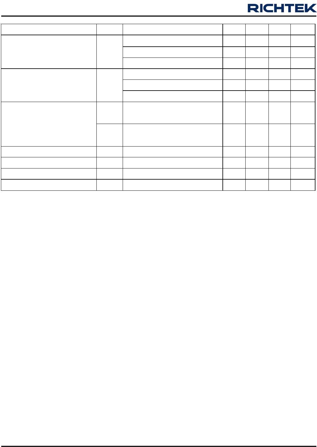
Parameter Symbol Test Conditions Min Typ Max Unit
f =100Hz -- 65 -- dB
f =1kHz -- 60 -- dB
PSRR
Loading=10mA
PSRR
f =10kHz -- 50 -- dB
f =100Hz -- 65 -- dB
f =1kHz -- 50 -- dB
PSRR
Loading=150mA
PSRR
f =10kHz -- 50 -- dB
V
THL
Low Threshold, % of nominal V
OU T
(Flag On)
90 -- -- %
Reset Threshol d
V
THH
High Threshold, % of nominal V
OU T
(Flag Off)
-- -- 96 %
POR Output Logic Low Voltage V
POR_L
I
L
= 250μA -- 0.02 0.1 V
POR Leakage Current I
POR
Flag off 1 0.01 1 μA
Set pin current source V
SET
= 0 0.60 1.25 1.70 μA
Set pin threshold POR = high -- 1.4 -- V
RT9010
5
DS9010-05 April 2011 www.richtek.com
Typical Operating Characteristics
Output Voltage vs. Temperature
1.7
1.75
1.8
1.85
1.9
-50 -25 0 25 50 75 100 125
Temperature
Output Voltage (V)
RT9010-18
(°C)
Output Voltage vs. Temperature
3.2
3.25
3.3
3.35
3.4
-50 -25 0 25 50 75 100 125
Temperature
Output Voltage (V)
RT9010-33
(°C)
Dropout Voltage vs. Load Current
0
50
100
150
200
250
300
350
0 50 100 150 200 250 300
Load Current (mA)
Dropout Voltage (mV)
RT9010-33
T
J
= 25°C
T
J
= -40°C
T
J
= 125°C
Quiescent Current vs. Temperature
50
55
60
65
70
-50 -25 0 25 50 75 100 125
Temperature
Quiescent Current (uA)
RT9010-33
V
IN
= V
EN
= 4.3V
C
IN
= C
OUT
1uF/X7R
(°C)
POR Delay
0.01
0.1
1
10
100
1000
10000
0.0001 0.0010 0.0100 0.1000 1.0000
POR Setting Capacitance (uF)
POR Delay Time (ms)
RT9010-28
0.0001 0.001 0.01 0.1 1
PSRR
-80
-60
-40
-20
0
20
10 100 1000 10000 100000 1000000
Frequency (Hz)
PSRR (dB)
I
LOAD
= 100mA
I
LOAD
= 10mA
I
LOAD
= 50mA
RT9010-15
V
IN
= 4.3V ± 0.1V
C
IN
= C
OUT
1uF/X7R
0.01 0.1 1 10k 100k 1000k
(Hz)
RT9010
6
DS9010-05 April 2011www.richtek.com
Load Transient Response
Time (250μs/Div)
I
OUT
(50mA/Div)
V
OUT
(20mV/Div)
RT9010-33, I
LOAD
= 10mA to 50mA
V
IN
= V
EN
= 4.3V
C
IN
= C
OUT
= 1uF/X7R
Load Transient Response
Time (250μs/Div)
I
OUT
(100mA/Div)
V
OUT
(20mV/Div)
RT9010-33, I
LOAD
= 10mA to 100mA
V
IN
= V
EN
= 4.3V
C
IN
= C
OUT
= 1uF/X7R
RT9010-28, Both I
LOAD
= 100mA
V
IN
= 3.8V to 4.8V
Line Transient Response
Time (100μs/Div)
V
OUT
(10mV/Div)
4.8
3.8
V
IN
(V)
RT9010-28, Both I
LOAD
= 50mA
V
IN
= 3.8V to 4.8V
Line Transient Response
Time (100μs/Div)
4.8
3.8
V
OUT
(10mV/Div)
V
IN
(V)
RT9010-28, Both I
LOAD
= 1mA
V
IN
= 3.8V to 4.8V
Line Transient Response
V
IN
(V)
Time (100μs/Div)
4.8
3.8
V
OUT
(10mV/Div)
RT9010-28, Both I
LOAD
= 10mA
V
IN
= 3.8V to 4.8V
Line Transient Response
V
IN
(V)
Time (100μs/Div)
4.8
3.8
V
OUT
(10mV/Div)

RT9010-12GJ6

Mfr. #:
Manufacturer:
Description:
IC REG LIN 1.2V 300MA TSOT23-6
Lifecycle:
New from this manufacturer.
Delivery:
DHL FedEx Ups TNT EMS
Payment:
T/T Paypal Visa MoneyGram Western Union

Products related to this Datasheet