NCP1215
http://onsemi.com
13
Figure 24 shows CT voltage and also by Channel 2 the
switch’s drain voltage at light load conditions.
Figure 24. CT and Drain at Light Load
The waveform on the current sense pin at full load
conditions can be observed from Channel 3 in Figure 25.
Figure 25. CS Pin at Full Load Condition
Figure 26 demonstrates the reduction of the peak primary
current at light load conditions.
Figure 26. CS Pin at Light Load Condition
Gate−Source Resistor Design Guidelines
In some applications, there is a need to wire a resistor
between the MOSFET gate and source connections. This
can preclude an eventual MOSFET destruction if, in the
production stage, the converter is powered whilst the gate is
left unconnected. However, dealing with an extremely low
startup current implies a careful selection of the gate−source
resistance. With the NCP1215, the gate−source resistor must
be calculated to allow the growth of the V
CC
capacitor to
4.0 V in order to not interfere with the power−on sequence.
The following equation helps deriving Rgate−source,
accounting for the minimum rectified input voltage and the
startup resistor: Vin
min
x Rgate−source/(Rgate−source +
Rstartup) u 4.0 V. If we take a Vin
min
of 100 VDC, a startup
resistor of 4.0 MW, then Rgate−source equals 180 kW as a
minimum normalized value.
NCP1215
http://onsemi.com
14
PACKAGE DIMENSIONS
SOIC−8
D SUFFIX
CASE 751−07
ISSUE AG
SEATING
PLANE
1
4
58
N
J
X 45
_
K
NOTES:
1. DIMENSIONING AND TOLERANCING PER
ANSI Y14.5M, 1982.
2. CONTROLLING DIMENSION: MILLIMETER.
3. DIMENSION A AND B DO NOT INCLUDE
MOLD PROTRUSION.
4. MAXIMUM MOLD PROTRUSION 0.15 (0.006)
PER SIDE.
5. DIMENSION D DOES NOT INCLUDE DAMBAR
PROTRUSION. ALLOWABLE DAMBAR
PROTRUSION SHALL BE 0.127 (0.005) TOTAL
IN EXCESS OF THE D DIMENSION AT
MAXIMUM MATERIAL CONDITION.
6. 751−01 THRU 751−06 ARE OBSOLETE. NEW
STANDARD IS 751−07.
A
B
S
D
H
C
0.10 (0.004)
DIM
A
MIN MAX MIN MAX
INCHES
4.80 5.00 0.189 0.197
MILLIMETERS
B 3.80 4.00 0.150 0.157
C 1.35 1.75 0.053 0.069
D 0.33 0.51 0.013 0.020
G 1.27 BSC 0.050 BSC
H 0.10 0.25 0.004 0.010
J 0.19 0.25 0.007 0.010
K 0.40 1.27 0.016 0.050
M 0 8 0 8
N 0.25 0.50 0.010 0.020
S 5.80 6.20 0.228 0.244
−X−
−Y−
G
M
Y
M
0.25 (0.010)
−Z−
Y
M
0.25 (0.010) Z
S
X
S
M
____
1.52
0.060
7.0
0.275
0.6
0.024
1.270
0.050
4.0
0.155
ǒ
mm
inches
Ǔ
SCALE 6:1
*For additional information on our Pb−Free strategy and soldering
details, please download the ON Semiconductor Soldering and
Mounting Techniques Reference Manual, SOLDERRM/D.
SOLDERING FOOTPRINT*
NCP1215
http://onsemi.com
15
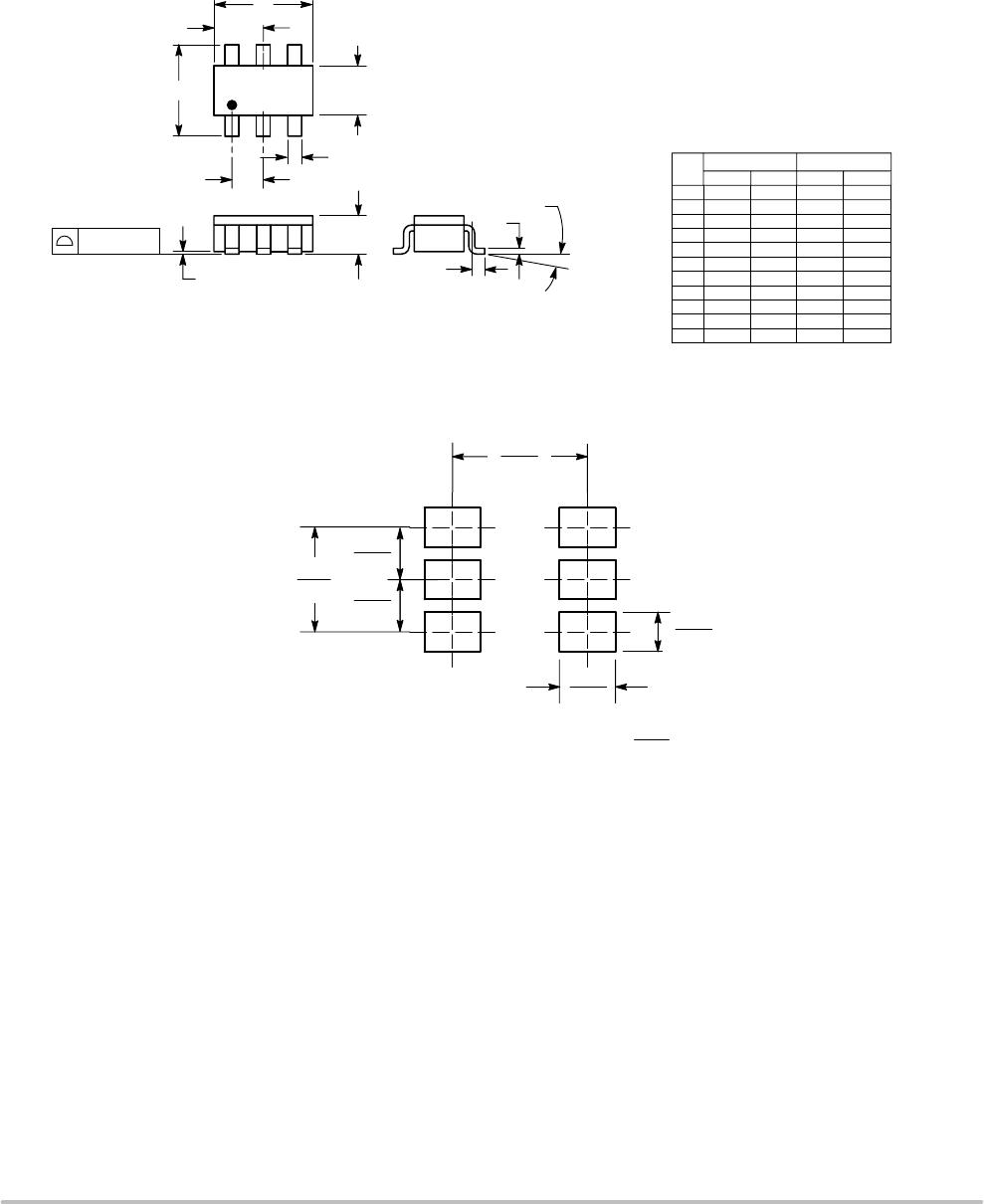
PACKAGE DIMENSIONS
TSOP−6
CASE 318G−02
ISSUE M
0.95
0.037
1.9
0.075
0.95
0.037
ǒ
mm
inches
Ǔ
SCALE 10:1
1.0
0.039
2.4
0.094
0.7
0.028
23
456
A
L
1
S
G
D
B
H
C
0.05 (0.002)
DIM MIN MAX MIN MAX
INCHESMILLIMETERS
A 0.1142 0.12202.90 3.10
B 0.0512 0.06691.30 1.70
C 0.0354 0.04330.90 1.10
D 0.0098 0.01970.25 0.50
G 0.0335 0.04130.85 1.05
H 0.0005 0.00400.013 0.100
J 0.0040 0.01020.10 0.26
K 0.0079 0.02360.20 0.60
L 0.0493 0.06101.25 1.55
M 0 10 0 10
S 0.0985 0.11812.50 3.00
__ __
NOTES:
1. DIMENSIONING AND TOLERANCING PER
ANSI Y14.5M, 1982.
2. CONTROLLING DIMENSION: MILLIMETER.
3. MAXIMUM LEAD THICKNESS INCLUDES
LEAD FINISH THICKNESS. MINIMUM LEAD
THICKNESS IS THE MINIMUM THICKNESS
OF BASE MATERIAL.
4. DIMENSIONS A AND B DO NOT INCLUDE
MOLD FLASH, PROTRUSIONS, OR GATE
BURRS.
M
J
K
*For additional information on our Pb−Free strategy and soldering
details, please download the ON Semiconductor Soldering and
Mounting Techniques Reference Manual, SOLDERRM/D.
SOLDERING FOOTPRINT*

NCP1215DR2

Mfr. #:
Manufacturer:
ON Semiconductor
Description:
Switching Controllers ANA VARIABL OFF TIME SMPS
Lifecycle:
New from this manufacturer.
Delivery:
DHL FedEx Ups TNT EMS
Payment:
T/T Paypal Visa MoneyGram Western Union

Products related to this Datasheet