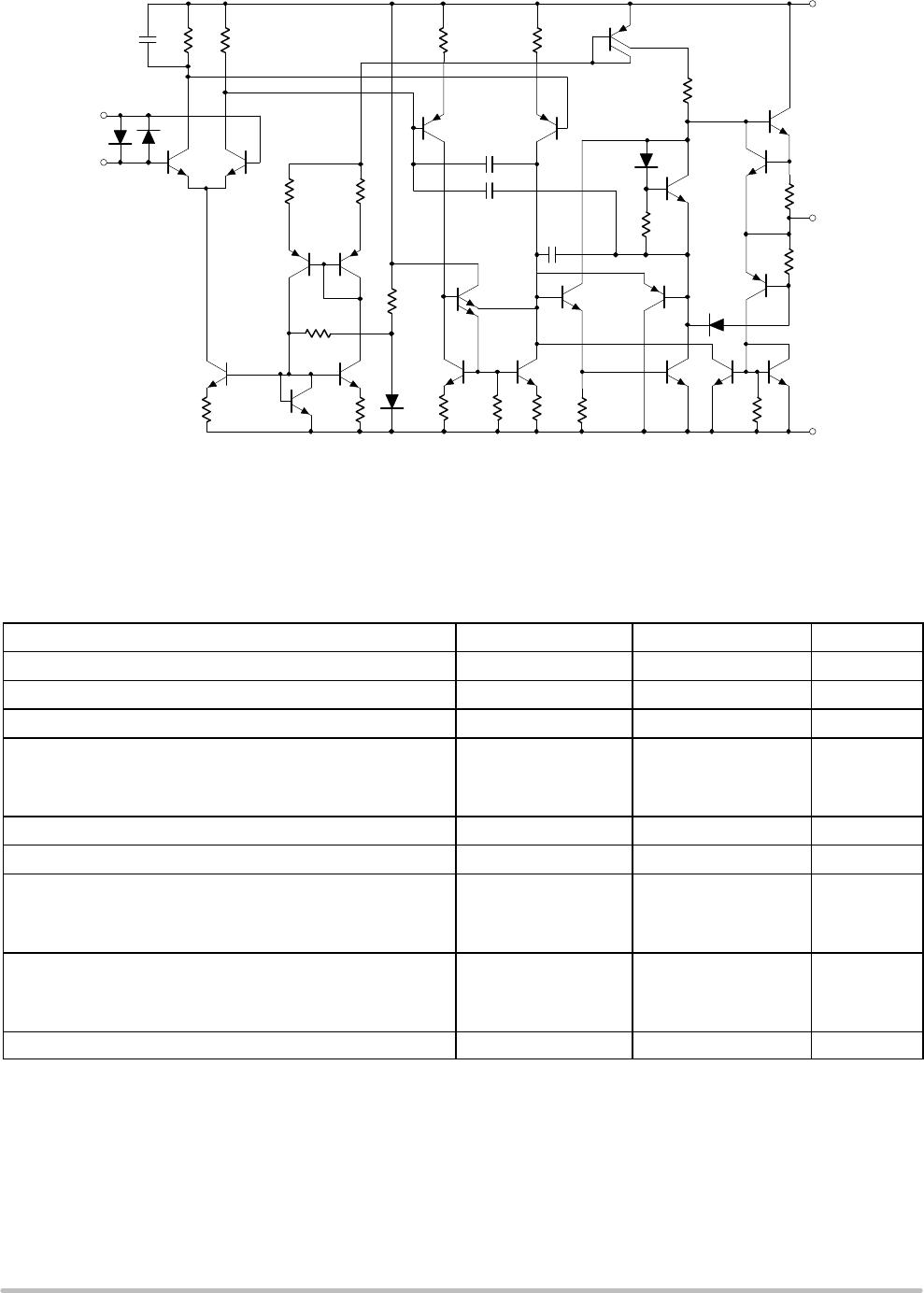
NE5532, SA5532, SE5532, NE5532A, SE5532A
http://onsemi.com
3
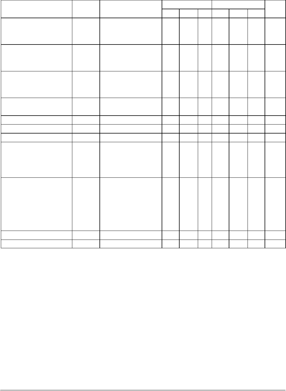
DC ELECTRICAL CHARACTERISTICS (T
amb
= 25°C; V
S
= "15 V, unless otherwise noted.) (Notes 2, 3 and 4)
Characteristic Symbol Test Conditions
SE5532/A NE5532/A, SA5532
Unit
Min Typ Max Min Typ Max
Offset Voltage V
OS
− − 0.5 2.0 − 0.5 4.0 mV
− Overtemperature − − 3.0 − − 5.0 mV
DV
OS
/DT − − 5.0 − − 5.0 − mV/°C
Offset Current I
OS
− − − 100 − 10 150 nA
− Overtemperature − − 200 − − 200 nA
DI
OS
/DT − − 200 − − 200 − pA/°C
Input Current I
B
− − 300 500 − 300 800 nA
− Overtemperature − − 700 − − 1000 nA
DI
B
/DT − − 5.0 − − 5.0 − nA/°C
Supply Current I
CC
− − 8.0 10.5 − 8.0 16 mA
− Overtemperature − − 13 − − −
Common-Mode Input Range V
CM
− "12 "13 − "12 "13 − V
Common-Mode Rejection Ratio CMRR − 80 100 − 70 100 − dB
Power Supply Rejection Ratio PSRR − − 10 50 − 10 100 mV/V
Large-Signal Voltage Gain A
VOL
R
L
w 2.0 kW; V
O
= "10 V 50 100 − 25 100 − V/mV
Overtemperature 25 − − 15 − −
R
L
w 600 W; V
O
= "10 V 40 50 − 15 50 −
Overtemperature 20 − − 10 − −
Output Swing V
OUT
R
L
w 600 W "12 "13 − "12 "13 − V
Overtemperature "10 "12 − "10 "12 −
R
L
w 600 W; V
S
= "18 V "15 "16 − "15 "16 −
Overtemperature "12 "14 − "12 "14 −
R
L
w 2.0 kW "13 "13.5 − "13 "13.5 −
Overtemperature "12 "12.5 − "10 "12.5 −
Input Resistance R
IN
− 30 300 − 30 300 − kW
Output Short Circuit Current I
SC
− 10 38 60 10 38 60 mA
2. Diodes protect the inputs against overvoltage. Therefore, unless current-limiting resistors are used, large currents will flow if the differential input
voltage exceeds 0.6 V. Maximum current should be limited to "10 mA.
3. For operation at elevated temperature, derate packages based on the package thermal resistance.
4. Output may be shorted to ground at V
S
= "15 V, T
amb
= 25°C. Temperature and/or supply voltages must be limited to ensure dissipation rating
is not exceeded.