LT8302
16
8302fc
For more information www.linear.com/LT8302
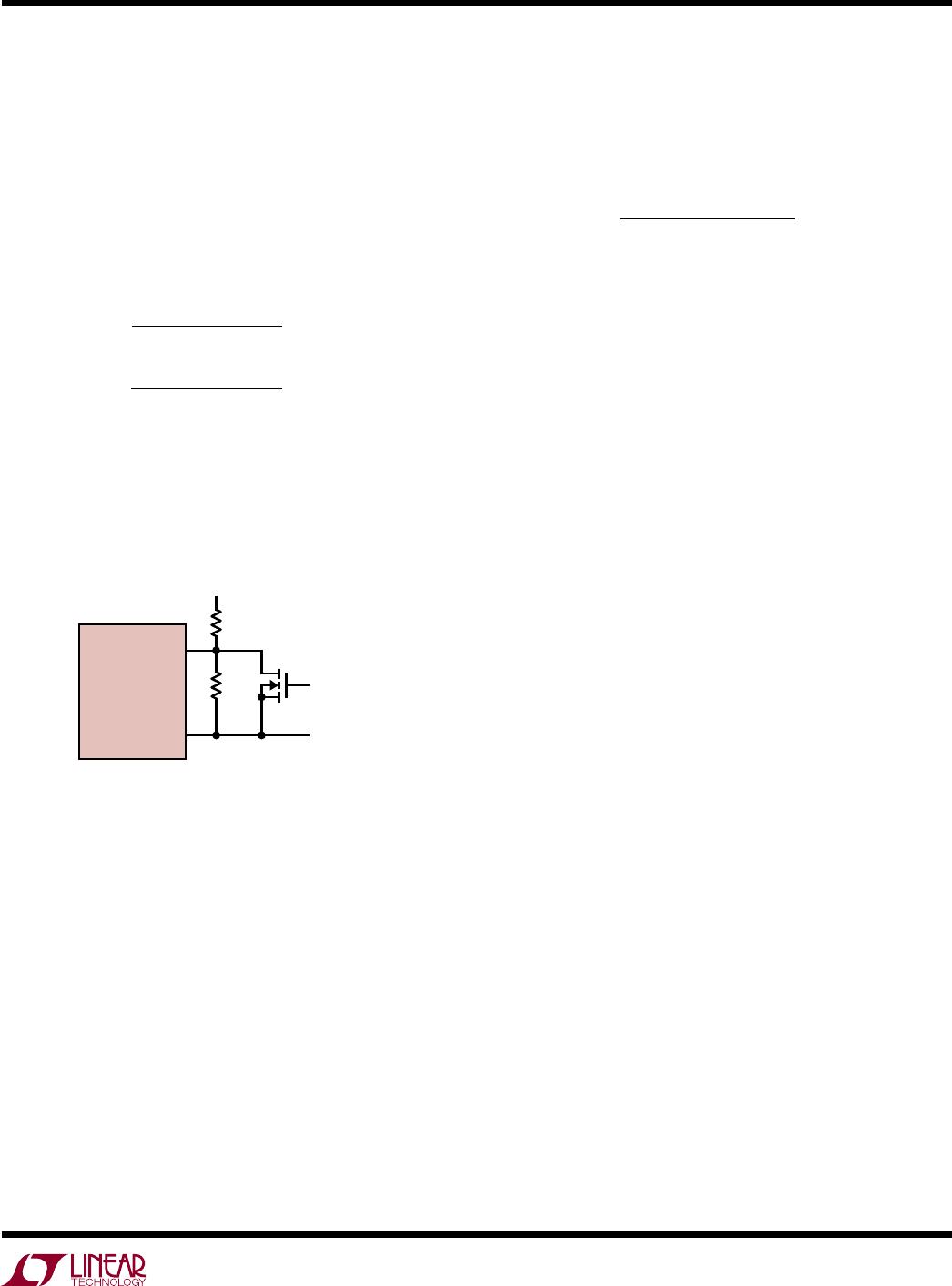
applicaTions inForMaTion
t
OFF
> 350ns
V
LEAKAGE
V
SW
<65V
<50V
TIME
8302 F05
t
SP
< 250ns
Figure 5. Maximum Voltages for SW Pin Flyback Waveform
In addition to the voltage spikes, the leakage inductance
also causes the SW pin ringing for a while after the power
switch turns off. To prevent the voltage ringing falsely trig
-
ger boundary mode detector, the LT8302 internally blanks
the boundary mode detector for approximately 250ns.
Any remaining voltage ringing after 250ns may turn the
power switch back on again before the secondary current
falls to zero. In this case, the LT8302 enters continuous
conduction mode. So the leakage inductance spike ringing
should be limited to less than 250ns.
To clamp and damp the leakage voltage spikes, a
(RC + DZ) snubber
circuit
in Figure6 is recommended.
The RC (resistor-capacitor) snubber quickly damps the
voltage spike ringing and provides great load regulation
and EMI performance. And the DZ (diode-Zener) ensures
well defined and consistent clamping voltage to protect
SW pin from exceeding its 65V absolute maximum rating.
Figure 6. (RC + DZ) Snubber Circuit
8302 F06
R
CZ
D
L
ℓ
•
•
then add capacitance until the period of the ringing is 1.5
to 2 times longer. The change in period determines the
value of the parasitic capacitance, from which the para
-
sitic inductance can be also determined from the initial
period. Once the value of the SW node capacitance and
inductance is known, a series resistor can be added to
the snubber capacitance to dissipate power and critically
damp the ringing. The equation for deriving the optimal
series resistance using the observed periods ( t
PERIOD
and
t
PERIOD(SNUBBED)
) and snubber capacitance (C
SNUBBER
) is:
C
PAR
=
SNUBBER
t
PERIOD(SNUBBED)
t
PERIOD
⎛
⎝
⎜
⎞
⎠
⎟
2
–
L
PAR
=
t
PERIOD
2
C
PAR
• 4π
2
R
SNUBBER
=
L
PAR
C
PAR
Note that energy absorbed by the RC snubber will be
converted to heat and will not be delivered to the load.
In high voltage or high current applications, the snubber
needs to be sized for thermal dissipation. A 470pF capaci
-
tor in series with a 39Ω resistor is a good starting point.
For the DZ
snubber, proper care should be taken when
choosing both the diode and the Zener diode. Schottky
diodes are typically the best choice, but some PN diodes
can be used if they turn on fast enough to limit the leak
-
age inductance
spike. Choose
a diode that has a reverse-
voltage rating higher than the maximum SW pin voltage.
The Zener diode breakdown voltage should be chosen to
balance power loss and switch voltage protection. The best
compromise is to choose the largest voltage breakdown
with 5V margin. Use the following equation to make the
proper choice:
V
ZENNER(MAX)
≤ 60V – V
IN(MAX)
For an application with a maximum input voltage of 32V,
choose a 24V Zener diode, the V
ZENER(MAX)
of which is
around 26V and below the 28V maximum. The power loss
in the DZ snubber determines the power rating of the Zener
diode. A 1.5W Zener diode is typically recommended.
The recommended approach for designing an RC snub-
ber is to measure the period of the ringing on the SW pin
when the power
switch turns off without the snubber and