11
IDT70V659/58/57S
High-Speed 3.3V 128/64/32K x 36 Asynchronous Dual-Port Static RAM Industrial and Commercial Temperature Ranges
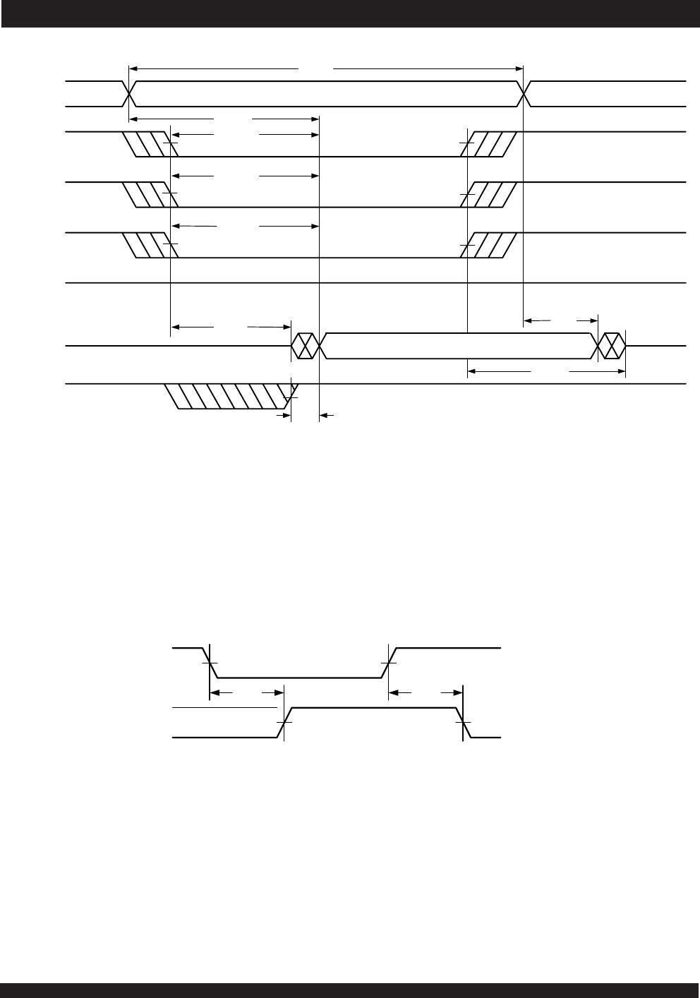
AC Electrical Characteristics Over the
Operating Temperature and Supply Voltage Range
(5)
NOTES:
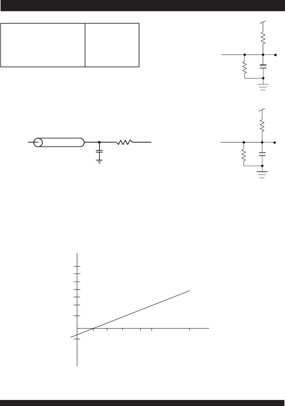
1. Transition is measured 0mV from Low or High-impedance voltage with Output Test Load (Figure 2).
2. This parameter is guaranted by device characterization, but is not production tested.
3. To access RAM, CE= V
IL and SEM = VIH. To access semaphore, CE = VIH and SEM = VIL. Either condition must be valid for the entire tEW time.
4. The specification for t
DH must be met by the device supplying write data to the RAM under all operating conditions. Although tDH and tOW values will vary over voltage
and temperature, the actual t
DH will always be smaller than the actual tOW.
5. These values are valid regardless of the power supply level selected for I/O and control signals (3.3V/2.5V). See page 6 for details.
AC Electrical Characteristics Over the
Operating Temperature and Supply Voltage
(5)
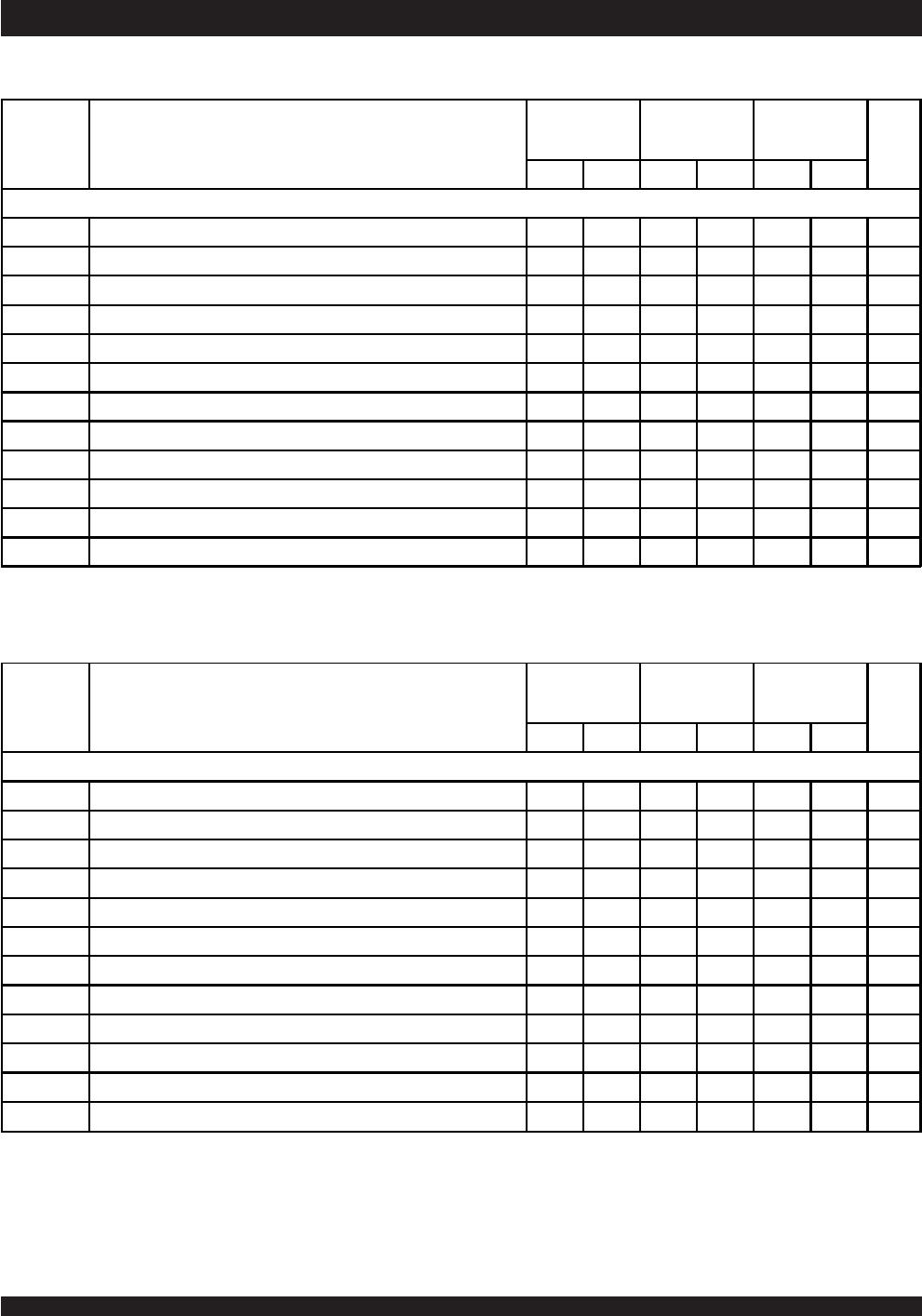
Symbol Parameter
70V659/58/57S10
Com'l Only
70V659/58/57S12
Com'l
& Ind
70V659/58/57S15
Com'l
& Ind
UnitMin. Max. Min. Max. Min. Max.
READ CYCLE
t
RC
Read Cycle Time 10
____
12
____
15
____
ns
t
AA
Address Access Time
____
10
____
12
____
15 ns
t
ACE
Chip Enable Access Time
(3)
____
10
____
12
____
15 ns
t
ABE
Byte Enable Access Time
(3)
____
5
____
6
____
7ns
t
AOE
Output Enable Access Time
____
5
____
6
____
7ns
t
OH
Output Hold from Address Change 3
____
3
____
3
____
ns
t
LZ
Output Low-Z Time
(1,2)
0
____
0
____
0
____
ns
t
HZ
Output High-Z Time
(1,2)
040608ns
t
PU
Chip Enable to Power Up Time
(2)
0
____
0
____
0
____
ns
t
PD
Chip Disable to Power Down Time
(2)
____
10
____
10
____
15 ns
t
SOP
Semaphore Flag Update Pulse (OE or SEM)
____
4
____
6
____
8ns
t
SAA
Semaphore Address Access Time 3 10 3 12 3 20 ns
4869 tbl 12
Symbol Parameter
70V659/58/57S10
Com'l Only
70V659/58/57S12
Com'l
& Ind
70V659/58/57S15
Com'l
& Ind
UnitMi n. Ma x. M in. M ax. Mi n. Ma x.
WRITE CYCLE
t
WC
Write Cycle Time 10
____
12
____
15
____
ns
t
EW
Chip Enable to End-of-Write
(3)
8
____
10
____
12
____
ns
t
AW
Address Valid to End-of-Write 8
____
10
____
12
____
ns
t
AS
Address Set-up Time
(3)
0
____
0
____
0
____
ns
t
WP
Write Pulse Width 8
____
10
____
12
____
ns
t
WR
Write Recovery Time 0
____
0
____
0
____
ns
t
DW
Data Valid to End-of-Write 6
____
8
____
10
____
ns
t
DH
Data Hold Time
(4)
0
____
0
____
0
____
ns
t
WZ
Write Enable to Output in High-Z
(1,2)
____
4
____
4
____
4ns
t
OW
Output Active from End-of-Write
(1,2,4)
0
____
0
____
0
____
ns
t
SWRD
SEM Flag Write to Read Time
5
____
5
____
5
____
ns
t
SPS
SEM Flag Contention Window
5
____
5
____
5
____
ns
4869 tbl 13