13
IDT70V659/58/57S
High-Speed 3.3V 128/64/32K x 36 Asynchronous Dual-Port Static RAM Industrial and Commercial Temperature Ranges
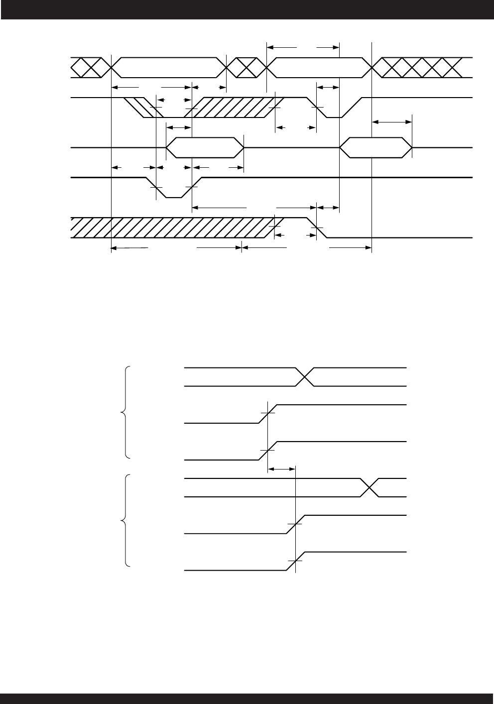
Timing Waveform of Write Cycle No. 1, R/W Controlled Timing
(1,5,8)
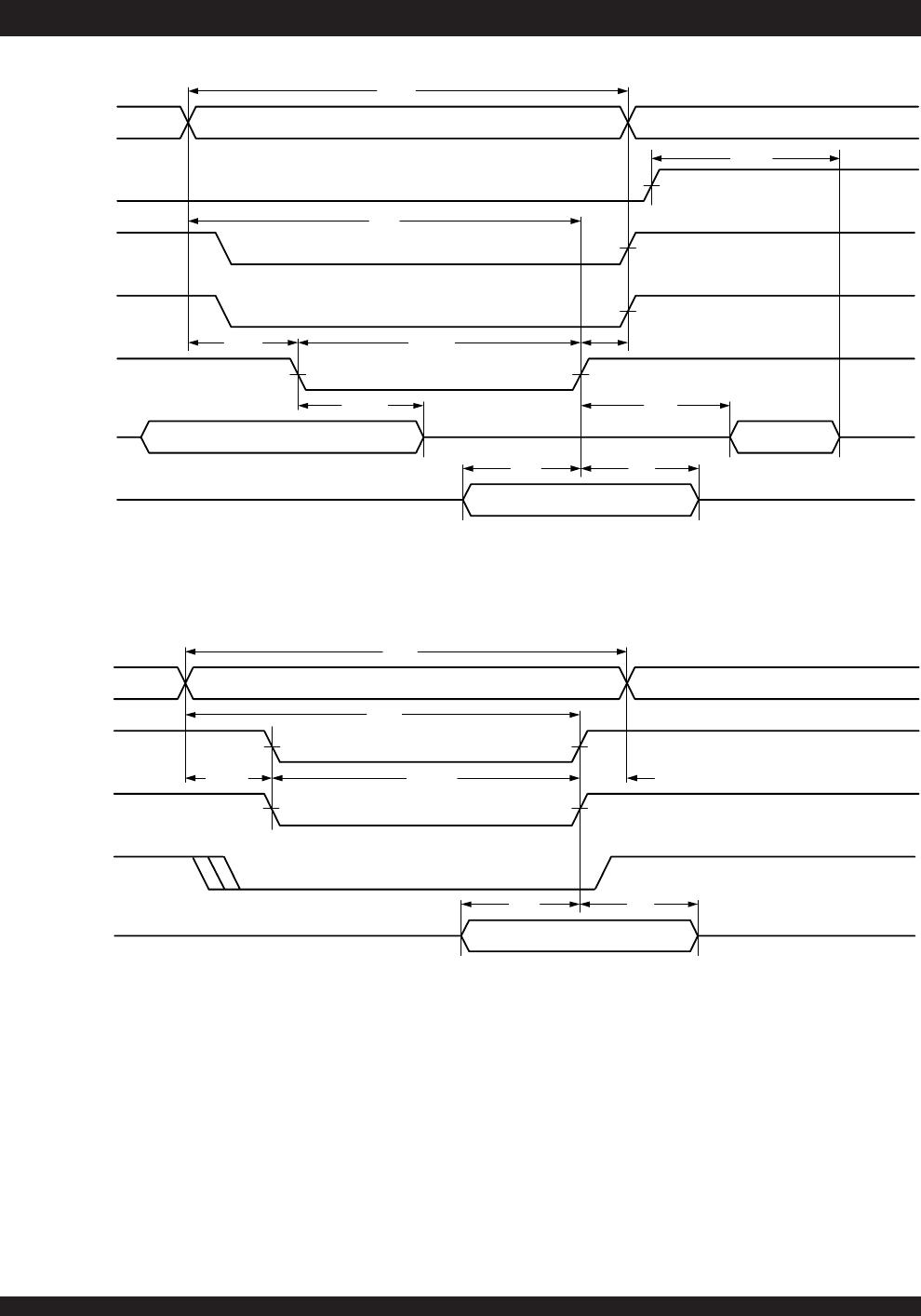
Timing Waveform of Write Cycle No. 2, CE Controlled Timing
(1,5)
NOTES:
1. R/W or CE or BEn = V
IH during all address transitions.
2. A write occurs during the overlap (t
EW or tWP) of a CE = VIL and a R/W = VIL for memory array writing cycle.
3. t
WR is measured from the earlier of CE or R/W (or SEM or R/W) going HIGH to the end of write cycle.
4. During this period, the I/O pins are in the output state and input signals must not be applied.
5. If the CE or SEM = V
IL transition occurs simultaneously with or after the R/W = VIL transition, the outputs remain in the High-impedance state.
6. Timing depends on which enable signal is asserted last, CE or R/W.
7. This parameter is guaranteed by device characterization, but is not production tested. Transition is measured 0mV from steady state with the Output Test Load
(Figure 2).
8. If OE = V
IL during R/W controlled write cycle, the write pulse width must be the larger of tWP or (tWZ + tDW) to allow the I/O drivers to turn off and data to be
placed on the bus for the required t
DW. If OE = VIH during an R/W controlled write cycle, this requirement does not apply and the write pulse can be as short as the
specified t
WP.
9. To access RAM, CE = V
IL and SEM = VIH. To access semaphore, CE = VIH and SEM = VIL. tEW must be met for either condition.
R/W
t
WC
t
HZ
t
AW
t
WR
t
AS
t
WP
DATA
OUT
(2)
t
WZ
t
DW
t
DH
t
OW
OE
ADDRESS
DATA
IN
(6)
(4) (4)
(7)
BEn
4869 drw 08
(9)
CE or SEM
(9)
(7)
(3)
4869 drw 09
t
WC
t
AS
t
WR
t
DW
t
DH
ADDRESS
DATA
IN
R/W
t
AW
t
EW
BEn
(3)
(2)
(6)
CE or SEM
(9)
(9)
.
IDT70V659/58/57S
High-Speed 3.3V 128/64/32K x 36 Asynchronous Dual-Port Static RAM Industrial and Commercial Temperature Ranges
14
Timing Waveform of Semaphore Read after Write Timing, Either Side
(1)
NOTES:
1. D
OR = DOL = VIL, CEL = CER = VIH. Refer to Truth Table II for appropriate BE controls.
2. All timing is the same for left and right ports. Port "A" may be either left or right port. "B" is the opposite from port "A".
3. This parameter is measured from R/W
"A" or SEM"A" going HIGH to R/W"B" or SEM"B" going HIGH.
4. If t
SPS is not satisfied,the semaphore will fall positively to one side or the other, but there is no guarantee which side will be granted the semaphore flag.
Timing Waveform of Semaphore Write Contention
(1,3,4)
NOTES:
1. CE = V
IH for the duration of the above timing (both write and read cycle) (Refer to Chip Enable Truth Table). Refer also to Truth Table II for appropriate BE controls.
2. "DATA
OUT VALID" represents all I/O's (I/O0 - I/O35) equal to the semaphore value.
SEM/BEn
(1)
4869 drw 10
t
AW
t
EW
I/O
VALID ADDRESS
t
SAA
R/W
t
WR
t
OH
t
ACE
VALID ADDRESS
DATA VALID
IN
DATA
OUT
t
DW
t
WP
t
DH
t
AS
t
SWRD
t
AOE
Read Cycle
Write Cycle
A
0
-A
2
OE
VALID
(2)
t
SOP
t
SOP
SEM
"A"
4869 drw 11
t
SPS
MATCH
R/W
"A"
MATCH
A
0"A"
-A
2"A"
SIDE "A"
(2)
SEM
"B"
R/W
"B"
A
0"B"
-A
2"B"
SIDE
"B"
(2)
.
15
IDT70V659/58/57S
High-Speed 3.3V 128/64/32K x 36 Asynchronous Dual-Port Static RAM Industrial and Commercial Temperature Ranges
NOTES:
1. Port-to-port delay through RAM cells from writing port to reading port, refer to "Timing Waveform of Write with Port-to-Port Read and BUSY (M/S = V
IH)".
2. To ensure that the earlier of the two ports wins.
3. t
BDD is a calculated parameter and is the greater of the Max. spec, tWDD – tWP (actual), or tDDD – tDW (actual).
4. To ensure that the write cycle is inhibited on port "B" during contention on port "A".
5. To ensure that a write cycle is completed on port "B" after contention on port "A".
AC Electrical Characteristics Over the
Operating Temperature and Supply Voltage Range
Symbol Parameter
70V659/58/57S10
Com'l Only
70V659/58/57S12
Com'l
& Ind
70V659/58/57S15
Com'l
& Ind
Unit
Min. Max. Min. Max. Min. Max.
BUSY TIMING (M/S=V
IH
)
t
BAA
BUSY Access Time from Address Match
____
10
____
12
____
15 ns
t
BDA
BUSY Disable Time from Address Not Matched
____
10
____
12
____
15 ns
t
BAC
BUSY Access Time from Chip Enable Low
____
10
____
12
____
15 ns
t
BDC
BUSY Disable Time from Chip Enable High
____
10
____
12
____
15 ns
t
APS
Arbitration Priority Set-up Time
(2)
5
____
5
____
5
____
ns
t
BDD
BUSY Disable to Valid Data
(3)
____
10
____
12
____
15 ns
t
WH
Write Hold After BUSY
(5)
8
____
10
____
12
____
ns
BUSY TIMING (M/S=V
IL
)
t
WB
BUSY Input to Write
(4)
0
____
0
____
0
____
ns
t
WH
Write Hold After BUSY
(5)
8
____
10
____
12
____
ns
PORT-TO-PORT DELAY TIMING
t
WDD
Write Pulse to Data Delay
(1)
____
22
____
25
____
30 ns
t
DDD
Write Data Valid to Read Data Delay
(1)
____
20
____
22
____
25 ns
4869 tbl 14

70V658S12BCI

Mfr. #:
Manufacturer:
IDT
Description:
SRAM 64Kx36 STD-PWR, 3.3V DUAL-PORT RAM
Lifecycle:
New from this manufacturer.
Delivery:
DHL FedEx Ups TNT EMS
Payment:
T/T Paypal Visa MoneyGram Western Union