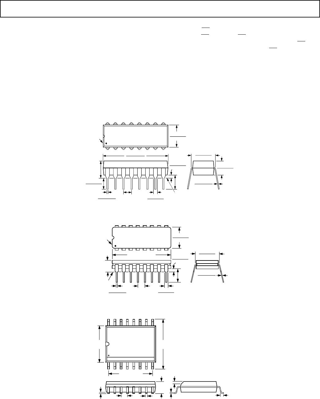
ADM696/ADM697
REV. 0–10–
Replacing the Back-Up Battery
When changing the back-up battery with system power on, spu-
rious resets can occur when the battery is removed. This occurs
because the leakage current flowing out of the V
BATT
pin will
charge up the stray capacitance. If the voltage on V
BATT
reaches
within 50 mV of V
CC
, a reset pulse is generated.
If spurious resets during battery replacement are acceptable,
then no action is required. If not, then one of the following solu-
tions should be considered:
1. A capacitor from V
BATT
to GND. This gives time while the
capacitor is charging up to change the battery. The leakage
current will charge up the external capacitor towards the
V
CC
level. The time taken is related to the charging current,
the size of external capacitor and the voltage differential be-
tween the capacitor and the charging voltage supply.
t = C
EXT
×
V
DIFF
/I
The maximum leakage (charging) current is 1 µA over tem-
perature and V
DIFF
= V
CC
V
BATT
. Therefore, the capacitor
size should be chosen such that sufficient time is available to
make the battery replacement.
C
EXT
= T
REQD
(1 µA/(V
CC
– V
BATT
))
If a replacement time of 5 s is allowed and assuming a V
CC
of 4.5 V and a V
BATT
of 3 V,
C
EXT
= 3.33
µ
F
2. A resistor from V
BATT
to GND. This will prevent the voltage
on V
BATT
from rising to within 50 mV of V
CC
during battery
replacement.
R = (V
CC
– 50 mV)/1 µA
Note that the resistor will discharge the battery slightly.
With a V
CC
supply of 4.5 V, a suitable resistor is 4.3 MΩ.
With a 3 V battery, this will draw around 700 nA. This will
be negligible in most cases.
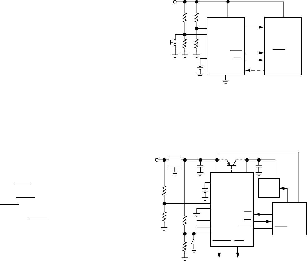
TYPICAL APPLICATIONS
ADM696
Figure 18 shows the ADM696 in a typical power monitoring,
battery backup application. V
OUT
powers the CMOS RAM.
Under normal operating conditions with V
CC
present, V
OUT
is
internally connected to V
CC
. If a power failure occurs, V
CC
will
decay and V
OUT
will be switched to V
BATT
, thereby maintaining
power for the CMOS RAM.
Power Fail RESET
The V
CC
power supply is also monitored by the Low Line In-
put, LL
IN
. A RESET pulse is generated when LL
IN
falls below
1.3 V.
RESET will remain low for 50 ms after LL
IN
returns
above 1.3 V. This allows for a power-on reset and prevents re-
peated toggling of
RESET if the V
CC
power supply is unstable.
Resistors R3 and R4 should be chosen to give the desired V
CC
reset threshold.
Watchdog Timer
The Watchdog Timer Input (WDI) monitors an I/O line from
the µP system. This line must be toggled once every 1.6 s to
verify correct software execution. Failure to toggle the line indi-
cates that the µP system is not correctly executing its program
and may be tied up in an endless loop. If this happens, a reset
pulse is generated to initialize the processor.
If the watchdog timer is not needed the WDI input should be
left floating.
Power Fail Detector
The Power Fail Input, PFI, monitors the input power supply via
a resistive divider network R1 and R2. This input is intended as
an early warning power fail input. The voltage on the PFI input
is compared with a precision 1.3 V internal reference. If the in-
put voltage drops below 1.3 V, a power fail output (PFO) signal
is generated. This warns of an impending power failure and may
be used to interrupt the processor so that the system may be
shut down in an orderly fashion. The resistors in the sensing
network are ratioed to give the desired power fail threshold volt-
age V
T
. The threshold should be set at a higher voltage than the
RESET threshold so that there is sufficient time available to
complete the shutdown procedure before the processor is
RESET and power is lost.
ADM696
R2
R1
PFO
+5V
V
CC
CMOS RAM
POWER
I/O LINE
µP NMI
µP RESET
µP SYSTEM
µP POWER
V
OUT
RESET
WDI
GND
PFI
V
BATT
BATTERY
+
R4
R3
LL
IN
RESET
Figure 18a. ADM696 Typical Application Circuit A
Figure 18b shows a similar application for the ADM696 but in
this case the PFI input monitors the unregulated input to the
7805 voltage regulator. This gives an earlier warning of an im-
pending power failure. It is useful with processors operating at
low speeds or where there are a significant number of house-
keeping tasks to be completed before the power is lost.
ADM696
R2
R1
PFO
INPUT
POWER
V
CC
V
OUT
WDI
GND
PFI
V
BATT
0.1µF
3V
BATTERY
RESET
OSC IN
OSC SEL
LOW LINE WDO
SYSTEM STATUS
INDICATORS
CMOS
RAM
I/O LINE
NMI
RESET
A0–A15
µP
BATT
ON
NC
V
CC
LL
IN
µP
POWER
RESET
R4
R3
7805
0.1µF
Figure 18b. ADM696 Typical Application Circuit B