LT4275BIDD#PBF

LT4275
7
4275f
applicaTions inForMaTion
Table 1. Classification Codes, Power Levels and Resistor Selection
CLASS
PD POWER
AVAILABLE PD TYPE
NOMINAL CLASS
CURRENT
LT4275 GRADE CAPABILITY RESISTOR
A B C R
CLS
R
CLS
++
0 13W Type 1 <0.4mA
Open Open
1 3.84W Type 1 10.5mA
140Ω Open
2 6.49W Type 1 18.5mA
76.8Ω Open
3 13W Type 1 28mA
49.9Ω Open
4 25.5W Type 2 40mA
34.8Ω Open
4* 38.7W LTPoE
++
40mA
Open 34.8Ω
4* 52.7W LTPoE
++
40mA
140Ω 46.4Ω
4* 70W LTPoE
++
40mA
76.8Ω 64.9Ω
4* 90W LTPoE
++
40mA
49.9Ω 118Ω
*An LTPoE
++
PD will be classified as class 4 by an IEEE 802.3 compliant PSE.
LT P oE
++
CLASSIFICATION
The LT4275A allows higher power allocation while main-
taining backwards compatibility with existing PSE systems
by extending the classification signaling of IEEE 802.3.
Linear Technology PSE controllers that are capable of
LTPoE
++
are listed in the Related Parts section. IEEE PSEs
will classify an LTPoE
++
PD as a Type 2 PD.
SIGNATURE CORRUPT DURING MARK
During the mark state, the LT4275 presents <11to the
port as required by the IEEE specification.
INRUSH AND POWERED ON
Once the PSE detects and optionally classifies the PD, the
PSE then powers on the PD. When the port voltage rises
above the V
HSON
threshold, it begins to source I
GPU
out of
the HSGATE pin. This current flows into an external capaci-
tor
(C
GATE
in Figure 3) that causes a voltage to ramp up the
gate of the external MOSFET. The external MOSFET acts as
a source follower and ramps the voltage up on the output
bulk capacitor (C
PORT
in Figure 3) thereby determining the
inrush current (I
INRUSH
in Figure 3).
To meet IEEE requirements, design I
INRUSH
to be approxi-
mately 100mA. See equation below:
I
INRUSH
= I
GPU
C
PORT
C
GATE
The LT4275 internal charge pump provides an N-channel
MOSFET solution, eliminating a larger and more costly
P-channel FET. The low R
DS(ON)
MOSFET also maximizes
LT4275A
HSGATE
GND
4275 F03
VPORT HSSRC
C
GATE
3.3k
+
C
PORT
VPORT
I
INRUSH
Figure 3. Programming I
INRUSH
power delivery and efficiency, reduces power and heat
dissipation, and eases thermal design.
The PWRGD pin is held low by its open drain output until
HSGATE charges up to approximately 7V above HSSRC.
The PWRGD pin is used to hold off the isolated power
supply until inrush is complete and the external MOSFET
is fully enhanced. The HSGATE pin will remain high and
the PWRGD pin pulled down until the port voltage falls
below V
HSOFF
or the AUX pin is above V
AUXT
.
AUXILIARY SUPPLY OVERRIDE
If the AUX pin is held above V
AUXT
, the LT4275 enters
auxiliary power supply override mode. In this mode
the signature resistor is disconnected, classification is
disabled, HSGATE is pulled down, and the PWRGD pin is
allowed to float. The T2P pin pulls down on the LT4275A/
LT4275B when no R
CLS
++
resistor is present. The T2P pin
alternates between pulling down and floating at f
T2P
on the
LT4275A when the R
CLS
++
resistor is present.
LT4275
8
4275f
applicaTions inForMaTion
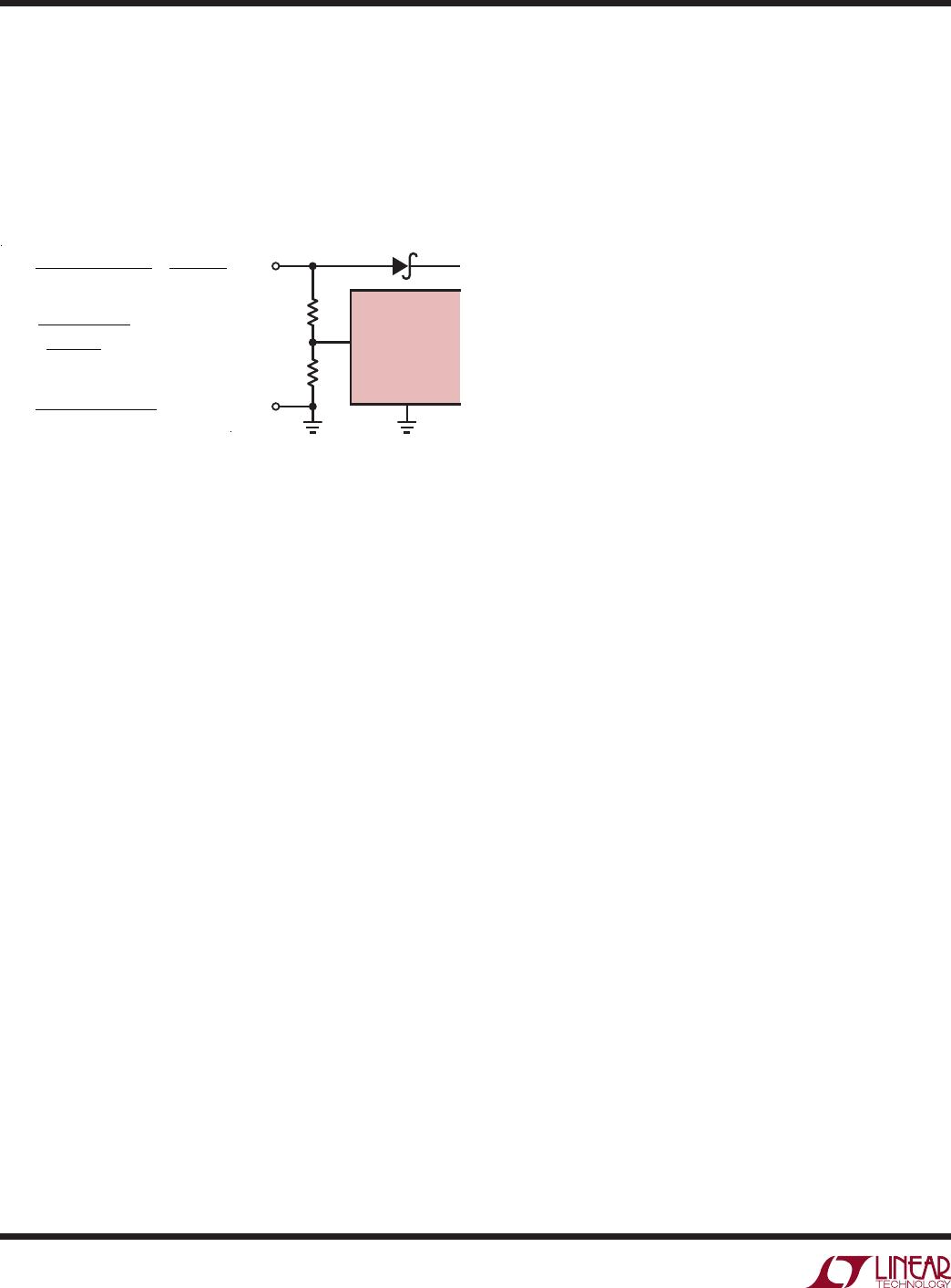
The AUX pin allows for setting the auxiliary supply turn on
(V
AUXON
) and turn off (V
AUXOFF
) voltage thresholds. The
auxiliary supply hysteresis voltage (V
AUXHYS
) is set by
sinking current (I
AUXH
) only when the AUX pin voltage is
less than V
AUXT
. Use the following equations to set V
AUXON
and V
AUXOFF
via R1 and R2 in Figure 4.
Figure 4. AUX Threshold and Hysteresis Calculation
Transient Voltage Suppressor
The LT4275 specifies an absolute maximum voltage of
100V and is designed to tolerate brief overvoltage events.
However, the pins that interface to the outside world can
routinely see excessive peak voltages. To protect the
LT4275, install a unidirectional transient voltage suppres-
sor (TVS) such as an SMAJ58A between the port voltage
and GND. This TVS must be mounted near the LT4275.
For extremely high cable discharge and surge protection
contact Linear Technology Applications.
Classification Resistor (R
CLS
and R
CLS
++
)
The R
CLS
resistors set the classification load current cor-
responding to the PD power classification. Select the value
of R
CLS
from Table 1 and connect the resistor between the
RCLASS pin and GND, or float the RCLASS pin if class 0
is required. The resistor tolerance must be 1% or better to
avoid
degrading the overall accuracy of the classification
circuit. For LTPoE
++
use the LT4275A and select the value
of R
CLS
++
from Table 1 in addition to R
CLS
.
Power Good Interface
The LT4275 provides a power good signal (PWRGD) to
simplify the isolated power supply design. The power good
signal is used to delay isolated power supply startup until
the C
PORT
capacitor is fully charged.
Exposed Pad
The LT4275A/LT4275B/LT4275C DFN package has an
exposed pad that is internally electrically connected to
GND. The exposed pad may only be connected to GND
on the printed circuit board.
LAYOUT CONSIDERATIONS
Avoid excessive parasitic capacitance on the RCLASS
pin and place resistor R
CLS
close to the LT4275. For the
LT4275A, place R
CLS
++ nearby as well.
It is strictly required for maximum protection to place the
input capacitor (C
PD
) and transient voltage suppressor as
close to the LT4275 as possible.
LT4275A
GND
4275 F04
AUX
R1
V
AUX
+
R2
R1=
V
AUXON
V
AUXOFF
I
AUXH
=
V
AUXHYS
I
AUXH
R2 =
R1
V
AUXOFF
V
AUXT
1
R1
V
AUX(MAX)
V
AUXT
1.4mA
THERMAL PROTECTION
The IEEE 802.3 specification requires a PD to withstand
any applied voltage from 0V to 57V indefinitely. During
classification, however, the power dissipation in the LT4275
may be as high as 1.5W. The LT4275 can easily tolerate
this power for the maximum IEEE timing but will overheat
if this condition persists abnormally.
The LT4275 includes a thermal protection feature which
protects itself from excessive heating. If the junction
temperature exceeds the overtemperature threshold, the
LT4275 pulls down the HSGATE and PWRGD pins and
disables classification.
EXTERNAL INTERFACE AND COMPONENT SELECTION
Input Diode Bridge
The input diode bridge introduces a voltage drop that affects
the voltage range for each mode of operation. The LT4275
is designed to tolerate these voltage drops. The voltages
shown in the Electrical Specifications are measured at the
LT4275 package pins.
Input Capacitor
A 0.1µF capacitor is needed from VPORT to GND to meet
an input impedance requirement in IEEE 802.3.
LT4275
9
4275f
Typical applicaTions
IEEE 802.3af (Type 1) 13W Powered Device
LT4275A/LT4275B/LT4275C
VPORT HSGATE
GND
4275 TA02
IEEEUVLO
HSSRC
RCLASS
RCLASS
++
PWRGD
T2P
AUX
R
CLS
C
PD
0.1µF
RUN
47nF
3.3k
FDN8601
SMAJ58A
V
IN
V
OUT
+
ISOLATED
POWER
SUPPLY
+
~
~
+
~
~
ETHERNET
MAGNETICS
C
PORT
V
PORT
LT4275A/LT4275B
VPORT HSGATE
GND
4275 TA03
IEEEUVLO
HSSRC
RCLASS
RCLASS
++
PWRGD
T2P
AUX
R
CLS
C
PD
0.1µF
RUN
47nF
3.3k
FDN8601
SMAJ58A
V
IN
V
OUT
+
ISOLATED
POWER
SUPPLY
OPTO
PSE TYPE
(TO µP)
+
~
~
+
~
~
ETHERNET
MAGNETICS
C
PORT
V
PORT
IEEE 802.3at (Type 2) 25.5W Powered Device
LTPoE
++
38.7W to 90W Powered Device
LT4275A
VPORT HSGATE
GND
4275 TA04
IEEEUVLO
HSSRC
RCLASS
RCLASS
++
R
CLS++
PWRGD
T2P
AUX
R
CLS
C
PD
0.1µF
RUN
47nF
3.3k
FDMC86102
SMAJ58A
V
IN
V
OUT
+
ISOLATED
POWER
SUPPLY
OPTO
PSE TYPE
(TO µP)
+
~
~
+
~
~
WÜRTH
749022016
+
C
PORT
V
PORT

LT4275BIDD#PBF

Mfr. #:
Manufacturer:
Analog Devices Inc.
Description:
Power Switch ICs - POE / LAN PoE+ PD Controller
Lifecycle:
New from this manufacturer.
Delivery:
DHL FedEx Ups TNT EMS
Payment:
T/T Paypal Visa MoneyGram Western Union