15
LTC1562
1562fa
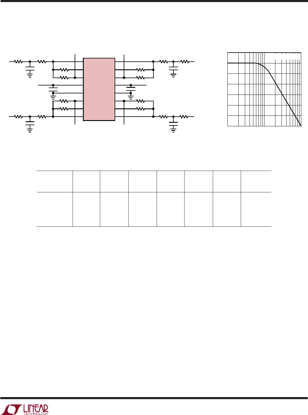
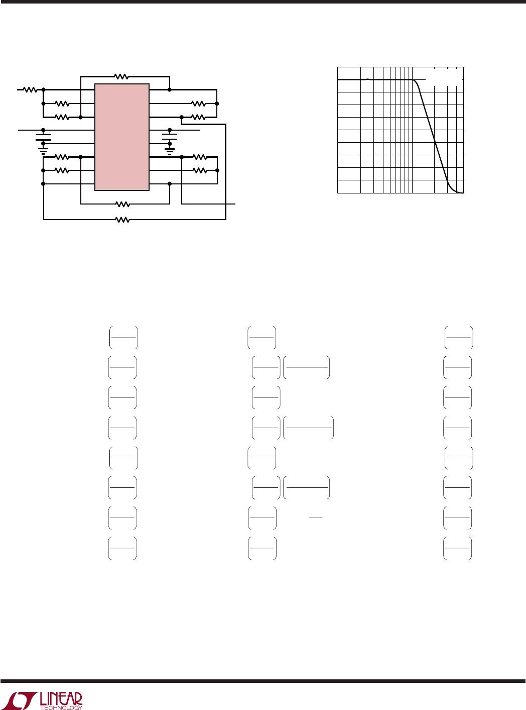
TYPICAL APPLICATIONS
U
(Basic)
8th Order Lowpass Filters Amplitude Response
R21 = R
IN1
= 10k
Quick Design Formulas for Some Popular Response Types:
2
100kHz
ƒ
C
Butterworth
(Maximally Flat Passband)
for f
C
10kHz to 140kHz
R21 = 7.51k , R
IN1
= 2.2R21*
, R
IN4
=
2
100kHz
ƒ
C
Chebyshev
(Equiripple Passband)
for f
C
20kHz to 120kHz
Bessel
(Good Transient Response)
for f
C
10kHz to 70kHz
R
Q1
= 6.01k
100kHz
ƒ
C
R
Q1
= 119.3k
100kHz
ƒ
C
100kHz
ƒ
C
+ 560kHz
100kHz
ƒ
C
+ 530kHz
R24*
2.2
100kHz
ƒ
C
+ 2440kHz
R22 = R
IN2
= 10k
2
100kHz
ƒ
C
R22 = R
IN2
= 14.99k
2
100kHz
ƒ
C
R
Q2
= 9k
Notes: f
C
is the cutoff frequency: For Butterworth and Bessel, response is 3dB down at f
C
. For Chebyshev filters with
±0.1dB passband ripple up to 0.95 f
C
, use LTC1562 “A” grade. *The resistor values marked with an asterisk (*) in the
Chebyshev formulas (R21 and R24) should be rounded to the nearest standard finite-tolerance value
before
computing
the values dependent on them (R
IN1
and R
IN4
respectively).
Example: Chebyshev response, f
C
= 100kHz. The formulas above give R21 = 7.51k, nearest standard 1% value 7.50k.
Using this 1% value gives R
IN1
= 16.5k, already a standard 1% value. R
Q1
= 18.075k, nearest 1% value 18.2k.
R22 = R
IN2
= 14.99k, nearest 1% value 15k. R
Q2
= 11.02k, nearest 1% value 11k. R23 = R
IN3
= 7.15k, already a
standard 1% value. R
Q3
= 18.75k, nearest 1% value 18.7k. R24 = 26.7k, already a standard 1% value. This gives
R
IN4
= 12.14k, nearest 1% value 12.1k. R
Q4
= 8.75k, nearest 1% value 8.66k.
100kHz
ƒ
C
R
Q2
= 279.9k
100kHz
ƒ
C
R23 = R
IN3
= 10k
2
100kHz
ƒ
C
R23 = R
IN3
= 7.15k
2
100kHz
ƒ
C
R
Q3
= 5.1k
100kHz
ƒ
C
R
Q3
= 118.1k
100kHz
ƒ
C
R24 = R
IN4
= 10k
2
100kHz
ƒ
C
R24 = 26.7k
2
100kHz
ƒ
C
R
Q4
= 25.63k
100kHz
ƒ
C
R21 = R
IN1
= 2.61k
2
100kHz
ƒ
C
R
Q1
= 3.63k
100kHz
ƒ
C
R22 = R
IN2
= 2.07k
2
100kHz
ƒ
C
R
Q2
= 5.58k
100kHz
ƒ
C
R23 = R
IN3
= 2.96k
2
100kHz
ƒ
C
R
Q3
= 3.05k
100kHz
ƒ
C
R24 = R
IN4
= 3.14k
2
100kHz
ƒ
C
R
Q4
= 2.84k
100kHz
ƒ
C
R
Q4
= 8.75k
100kHz
ƒ
C
1562 TA04 TABLE
1
2
3
5
6
8
9
10
20
19
18
16
15
13
12
11
INV B
V1 B
V2 B
V
+
SHDN
V2 A
V1 A
INV A
INV C
V1 C
V2 C
V
–
AGND
V2 D
V1 D
INV D
LTC1562
R
IN2
R
IN4
R
IN1
V
IN
V
OUT
1562 TA04a
R
IN3
–5V
5V
R
Q1
R21
R23
0.1µF
0.1µF
R
Q3
R24
R
Q4
R
Q2
R22
SCHEMATIC INCLUDES PIN NUMBERS FOR 20-PIN PACKAGE.
PINS 4, 7, 14, 17 (NOT SHOWN) ALSO CONNECT TO V
–
FREQUENCY (Hz)
GAIN (dB)
10
0
–10
–20
–30
–40
–50
–60
–70
–80
–90
10k 100k 500k
1562 TA04b
CHEBYSHEV
f
C
= 100kHz