19
M9999-122012
The voltage drop across R
SENSE
is sampled in such a
way that the high currents through the power traces will
not introduce significant parasitic voltage drops in the
sense leads. It is recommended to connect the hot swap
controller's sense leads directly to the sense resistor's
metalized contact pads. The Kelvin sense signal traces
should be symmetrical with equal length and width, kept
as short as possible and isolated from any noisy signals
and planes.
Figure 8. 4-Wire Kelvin Sense Connections for R
SENSE
Additionally, for designs that implement Kelvin sense
connections that exceed 1” in length and/or if the Kelvin
(signal) traces are vulnerable to noise possibly being
injected onto these signals, the example circuit shown in
Figure 9 can be implemented to combat noisy
environments. This circuit implements a 1.6 MHz low-
pass filter to attenuate higher frequency disturbances on
the current sensing circuitry. However, individual system
analysis should be used to determine if filtering is
necessary and to select the appropriate cutoff frequency
for each specific application.
Figure 9. Current-Limit Sense Filter for Noisy Systems
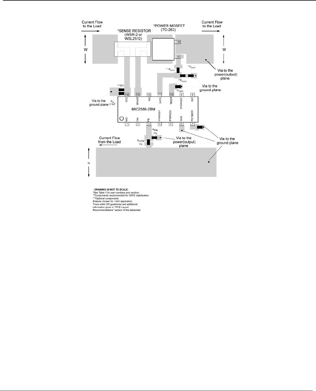
Other Layout Considerations
Figure 10 is a recommended PCB layout diagram for the
MIC2586-2BM. Many hot swap applications will require
load currents of several amperes. Therefore, the power
(V
CC
and Return) trace widths (W) need to be wide
enough to allow the current to flow while the rise in
temperature for a given copper plate (e.g., 1oz. or 2oz.)
is kept to a maximum of 10°C to 25°C. Also, these traces
should be as short as possible in order to minimize the
IR drops between the input and the load. The feedback
network resistor values in Figure 10 are selected for a
+24V application. The resistors for the feedback (FB)
and ON pin networks should be placed close to the
controller and the associated traces should be as short
as possible to improve the circuit’s noise immunity. The
input “clamping diode” (D1) is referenced in the typical
application circuit. If possible, use high-frequency PCB
layout techniques around the GATE circuitry (shown in
the typical application circuit) and use a dummy resistor
(e.g., R3 = 0Ω) during the prototype phase. If R3 is
needed to eliminate high-frequency oscillations, common
values for R3 range between 4.7Ω to 20Ω for various
power MOSFETs. Finally, the use of plated-through vias
will be needed to make circuit connection to the power
and ground planes when utilizing multi-layer PCBs.