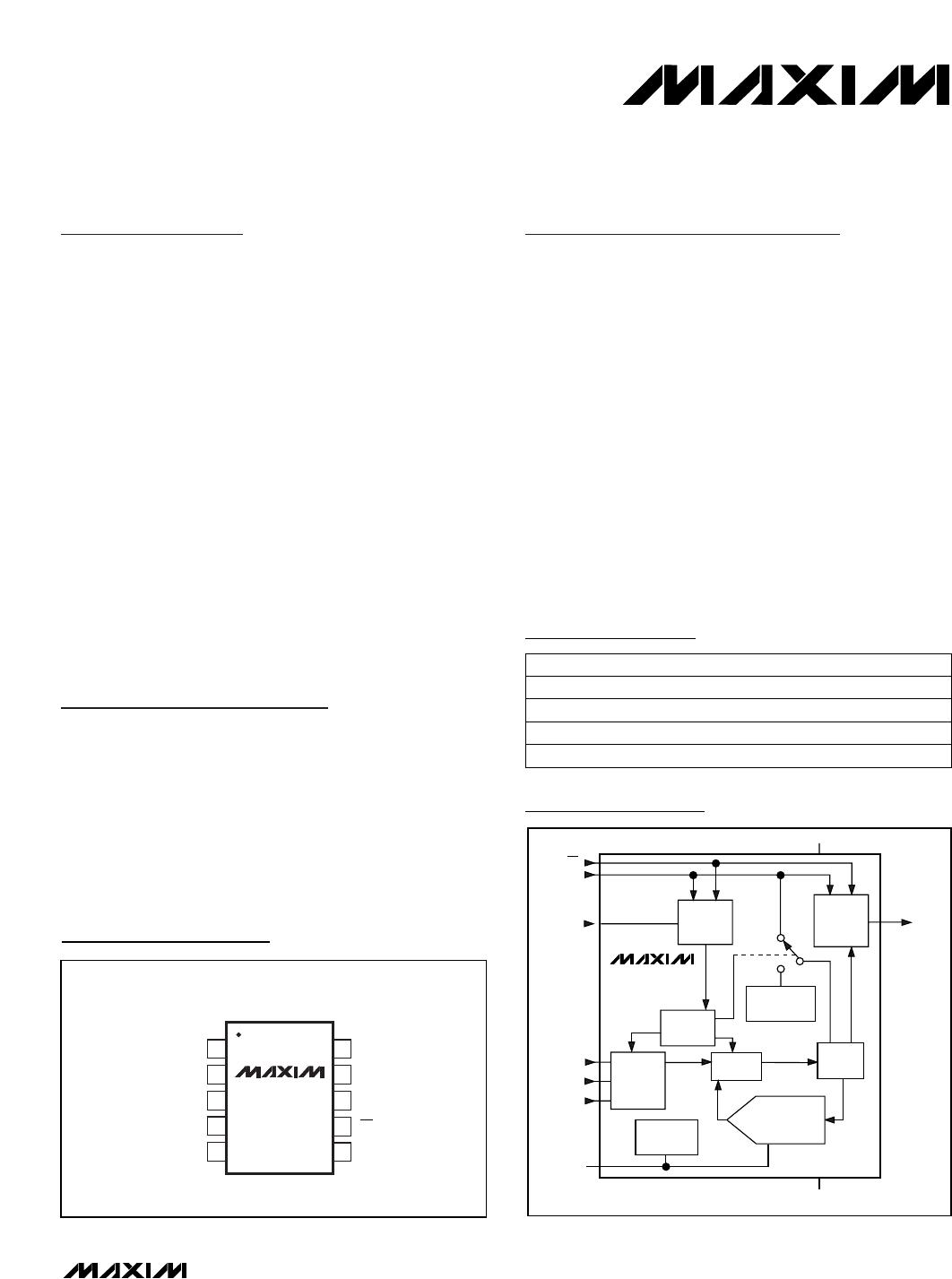
General Description
The MAX1108/MAX1109 low-power, 8-bit, dual-channel,
analog-to-digital converters (ADCs) feature an internal
track/hold (T/H) voltage reference, clock, and serial inter-
face. The MAX1108 is specified from +2.7V to +3.6V and
consumes only 105µA. The MAX1109 is specified from
+4.5V to +5.5V and consumes only 130µA. The analog
inputs are software configurable, allowing unipolar/bipolar
and single-ended/differential operation; battery monitor-
ing capability is also included.
The full-scale analog input range is determined by the
internal reference of +2.048V (MAX1108) or +4.096V
(MAX1109), or by an externally applied reference rang-
ing from 1V to V
DD
. The MAX1108/MAX1109 also feature
a software power-down mode that reduces power con-
sumption to 0.5µA when the device is not in use. The
4-wire serial interface directly connects to SPI™, QSPI™,
and MICROWIRE™ devices without external logic.
Conversions up to 50ksps are performed using either the
internal clock or an external serial-interface clock.
The MAX1108 and MAX1109 are available in a 10-pin
µMAX package with a footprint that is just 20% of an
8-pin plastic DIP.
Applications
Portable Data Logging
Hand-Held Measurement Devices
Medical Instruments
System Diagnostics
Solar-Powered Remote Systems
4–20mA-Powered Remote Systems
Receive-Signal Strength Indicators
Features
Single Supply: +2.7V to +3.6V (MAX1108)
+4.5V to +5.5V (MAX1109)
Low Power: 105µA at +3V and 50ksps
0.5µA in Power-Down Mode
Software-Configurable Unipolar or Bipolar Inputs
Input Voltage Range: 0 to V
DD
Internal Track/Hold
Internal Reference: +2.048V (MAX1108)
+4.096V (MAX1109)
Reference Input Range: 1V to V
DD
SPI/QSPI/MICROWIRE-Compatible Serial Interface
V
DD
Monitoring Mode
Small 10-Pin µMAX Package
MAX1108/MAX1109
Single-Supply, Low-Power,
2-Channel, Serial 8-Bit ADCs
________________________________________________________________ Maxim Integrated Products 1
1
2
3
4
5
10
9
8
7
6
SCLK
DOUT
DIN
CSGND
CH1
CH0
V
DD
MAX1108
MAX1109
µMAX
TOP VIEW
COMREF
INPUT
SHIFT
REGISTER
CONTROL
LOGIC
T/H
SAR
INTERNAL
OSCILLATOR
OUTPUT
SHIFT
REGISTER
V
DD
ANALOG
INPUT
MUX
INTERNAL
REFERENCE
DOUT
SCLK
DIN
CH0
COM
REF
CH1
CS
GND
CHARGE
REDISTRIBUTION
DAC
MAX1108
MAX1109
Functional Diagram
19-1399; Rev 1; 6/03
Pin Configuration
Ordering Information
PART
MAX1108CUB
MAX1108EUB -40°C to +85°C
0°C to +70°C
TEMP RANGE PIN-PACKAGE
10 µMAX
10 µMAX
MAX1109CUB
MAX1109EUB -40°C to +85°C
0°C to +70°C 10 µMAX
10 µMAX
SPI and QSPI are trademarks of Motorola, Inc. MICROWIRE is a trademark of National Semiconductor Corp.
For pricing, delivery, and ordering information, please contact Maxim/Dallas Direct! at
1-888-629-4642, or visit Maxim’s website at www.maxim-ic.com.
MAX1108/MAX1109
Single-Supply, Low-Power,
2-Channel, Serial 8-Bit ADCs
2 _______________________________________________________________________________________
ABSOLUTE MAXIMUM RATINGS
ELECTRICAL CHARACTERISTICS—MAX1108
(V
DD
= +2.7V to +3.6V; unipolar input mode; COM = GND, f
SCLK
= 500kHz, external clock mode (50% duty cycle); 10 clocks/conver-
sion cycle (50ksps); 1µF capacitor at REF, external +2.048V reference at REF; T
A
= T
MIN
to T
MAX
; unless otherwise noted. Typical
values are at T
A
= +25°C.)
Stresses beyond those listed under “Absolute Maximum Ratings” may cause permanent damage to the device. These are stress ratings only, and functional
operation of the device at these or any other conditions beyond those indicated in the operational sections of the specifications is not implied. Exposure to
absolute maximum rating conditions for extended periods may affect device reliability.
V
DD
to GND..............................................................-0.3V to +6V
CH0, CH1, COM, REF, DOUT to GND .......-0.3V to (V
DD
+ 0.3V)
DIN, SCLK, CS to GND ............................................-0.3V to +6V
Continuous Power Dissipation (T
A
= +70°C)
10-pin µMAX (derate 5.6mW/°C above +70°C) ............444mW
Operating Temperature Ranges
MAX110_CUB ......................................................0°C to +70°C
MAX110_EUB ...................................................-40°C to +85°C
Storage Temperature Range .............................-65°C to +150°C
Lead Temperature (soldering, 10s) .................................+300°C
V
DD
= 2.7V to 3.6V
V
DD
= 5.5V (Note 2)
No missing codes over temperature
CONDITIONS
±0.15 ±0.5
bits8Resolution
LSB
±0.2
INLRelative Accuracy (Note 1)
LSB±1DNLDifferential Nonlinearity
UNITSMIN TYP MAXSYMBOLPARAMETER
V
DD
= 5.5V (Note 2)
V
DD
= 2.7V to 3.6V
LSB
±0.5
Offset Error
±0.2 ±1
LSB±1Gain Error (Note 3)
ppm/°C±0.8Gain Temperature Coefficient
T
A
= T
MIN
to T
MAX
T
A
= +25°C
mV50V
DD
/ 2 Sampling Accuracy
dB49SINADSignal-to-Noise Plus Distortion
dB-70THD
Total Harmonic Distortion
(up to the 5th harmonic)
LSB
±0.5
TUETotal Unadjusted Error
±1
LSB±0.1
Channel-to-Channel
Offset Matching
-3dB rolloff
Unipolar input, V
COM
= 0
MHz0.8Full-Power Bandwidth
MHz1.5BW
-3dB
Small-Signal Bandwidth
0V
REF
Input Voltage Range (Note 4)
dB68SFDRSpurious-Free Dynamic Range
Bipolar input, V
COM
or V
CH1
= V
REF
/ 2,
referenced to COM or CH1
V
±V
REF
/ 2
V
CH_
pF18C
IN
Input Capacitance
On/off-leakage current,
V
COM
or V
CH
= 0 or V
DD
µA±0.01 ±1Multiplexer Leakage Current
DC ACCURACY
DYNAMIC PERFORMANCE (10kHz sine-wave input, 2.048Vp-p, 50ksps, 500kHz external clock)
ANALOG INPUTS
µA
MAX1108/MAX1109
Single-Supply, Low-Power,
2-Channel, Serial 8-Bit ADCs
_______________________________________________________________________________________ 3
ELECTRICAL CHARACTERISTICS—MAX1108 (continued)
(V
DD
= +2.7V to +3.6V; unipolar input mode; COM = GND, f
SCLK
= 500kHz, external clock mode (50% duty cycle); 10 clocks/conver-
sion cycle (50ksps); 1µF capacitor at REF, external +2.048V reference at REF; T
A
= T
MIN
to T
MAX
; unless otherwise noted. Typical
values are at T
A
= +25°C.)
CONDITIONS UNITSMIN TYP MAXSYMBOLPARAMETER
External clock, 500kHz, 10 sclks/conv
Internal clock
External clock, 2MHz
µs
20
t
CONV
Conversion Time (Note 5)
35
µs1t
ACQ
Track/Hold Acquisition Time
ps<50Aperture Jitter
ns10Aperture Delay
kHz400Internal Clock Frequency
(Note 6)
0 to 0.5mA (Note 7)
ppm/°C±50REF Tempco
µA150I
REFSC
REF Short-Circuit Current
mV2.5Load Regulation
kHz50 500
V1.968 2.048 2.128V
REF
Output Voltage
+2.048V at REF, full scale,
500kHz external clock
µA120Input Current
V2.7 3 5.5V
DD
Supply Voltage
Power down, V
DD
= 2.7V to 3.6V (Note 9)
Full-scale input, V
DD
= 2.7V to 3.6V
0.5 2.5
I
DD
mV±0.4 ±4PSRPower-Supply Rejection (Note 10)
V
DD
= 2.7V to 3.6V,
C
L
= 10pF
V
DD
= 5.5V,
C
L
= 10pF
105 250
130
µF1Capacitive Bypass at REF
V0.2V
HYST
Input Hysteresis
V0.8V
IL
Threshold Voltage Low
µA±1I
IH
Input Current High
V
DD
3.6V
V
DD
> 3.6V
V2
V3
V
IH
Threshold Voltage High
MHz2
External Clock Frequency Range
V1.0 V
DD
+ 0.05Input Voltage Range
µA±1I
IL
Input Current Low
pF15C
IN
Input Capacitance
For data transfer only
Internal reference
External reference 70
Internal reference
External reference 95
µASupply Current (Notes 2, 8)
TRACK/HOLD
INTERNAL REFERENCE
EXTERNAL REFERENCE
POWER REQUIREMENTS
DIGITAL INPUTS (DIN, SCLK, and CS)

MAX1109CUB+T

Mfr. #:
Manufacturer:
Maxim Integrated
Description:
Analog to Digital Converters - ADC 2Ch Single-Supply Low-P Serial 8-Bit
Lifecycle:
New from this manufacturer.
Delivery:
DHL FedEx Ups TNT EMS
Payment:
T/T Paypal Visa MoneyGram Western Union