DS1077L
4 of 21
TABLE 1
EN0
(BIT)
SEL0
(BIT)
PDN0
(BIT)
CTRL0
(PIN)
OUT0
(PIN)
CTRL0
FUNCTION
DEVICE
MODE
1
Hi-Z
(OUT1 and OUT2)
Power-Down
0 0 0
0 Hi-Z
Power-Down*
Active
1 Master Clk/M
0 1 0
0 Master Clk
MUX Select Active
1 Hi-Z
1 0 0
0 Master Clk
Output Enable Active
1 Hi-Z
1 1 0
0 Master Clk/M
Output Enable Active**
1
Hi-Z
(OUT1 and OUT2)
Power-Down
X
0
1
0 Master Clk
Power-Down
Active
1 Hi-Z Power-Down
X 1 1
0 Master Clk/M
Power-Down
Active
*This mode is for applications where OUT0 is not used, but CTRL0 is used as a device shutdown.
**Default Condition
CONTROL PIN 1 (CTRL1) – A multifunctional input pin that can be selected as an output enable
and/or a power-down. Its function is determined by the user-programmable control register value of
PDN1. (See Table 2.)
TABLE 2
PDN1
(BIT)
CTRL1
(PIN)
CTRL1
FUNCTION
OUT 1 DEVICE MODE
0 0 Output Enable Out Clk Active*
0 1 Output Enable Hi-Z Active*
1 0 Power-Down Out Clk Active
1 1 Power-Down
Hi-Z
(OUT1 and OUT2)
Power-Down
*Default Condition
NOTE:
Both CTRL0 and CTRL1 can be configured as power-downs, they are internally “OR” connected so that
either of the control pins may be used to provide a power-down function for the whole device, subject to
appropriate settings of the PDN0 and PDN1 register bits. (See Table 3.)
DS1077L
5 of 21
TABLE 3
PDN0
(BIT)
PDN1
(BIT)
SHUTDOWN CONTROL
0 0 None*
0 1 CTRL1
1 0 CTRL0
1 1 CTRL0 or CTRL1
*CTRL0 performs a power-down if SEL0 and EN0 are both 0. (See Table 1.)
Serial Data Input/Output (SDA) – Input/output pin for the 2-wire serial interface used for data transfer.
Serial Clock Input (SCL) – Input pin for the 2-wire serial interface used to synchronize data movement
on the serial interface.
REGISTER FUNCTIONS
The user-programmable registers can be programmed by the user to determine the mode of operation
(MUX), operating frequency (DIV) and bus settings (BUS). Details of how these registers are
programmed can be found in a later section; in this section the functions of the registers are described.
The register setting are nonvolatile, the values are stored automatically or as required in EEPROM when
the registers are programmed via the SDA and SCL pins.
MUX WORD
MSB LSB MSB LSB
Name
* PDN1 PDN0 SEL0 EN0 0M1 0M0 1M1 1M0 DIV1 - - - - - -
Default setting 0 0 0 1 1 0 0 0 0 0 x x x x x x
first data byte second data byte
*This bit must be set to zero.
DIV1 (bit)
This bit allows the output of the prescaler P1 to be routed directly to the OUT1 pin (DIV1 = 1). The N
divider is bypassed so the programmed value of N is ignored. If DIV1 = 0 (default) the N divider
functions normally.
0M1, 0M0, 1M1, 1M0 (bits)
These bits set the prescalers P0 and P1, to divide by 1, 2, 4, or 8. (See Table 4.)
TABLE 4
0M1 0M0
PRESCALER
P0 DIVISOR
“M”
1M1 1M0
PRESCALER
P1 DIVISOR
“M”
0 0
1*
0 0
1*
0 1 2 0 1 2
1 0 4 1 0 4
1 1 8 1 1 8
*Default Condition
DS1077L
6 of 21
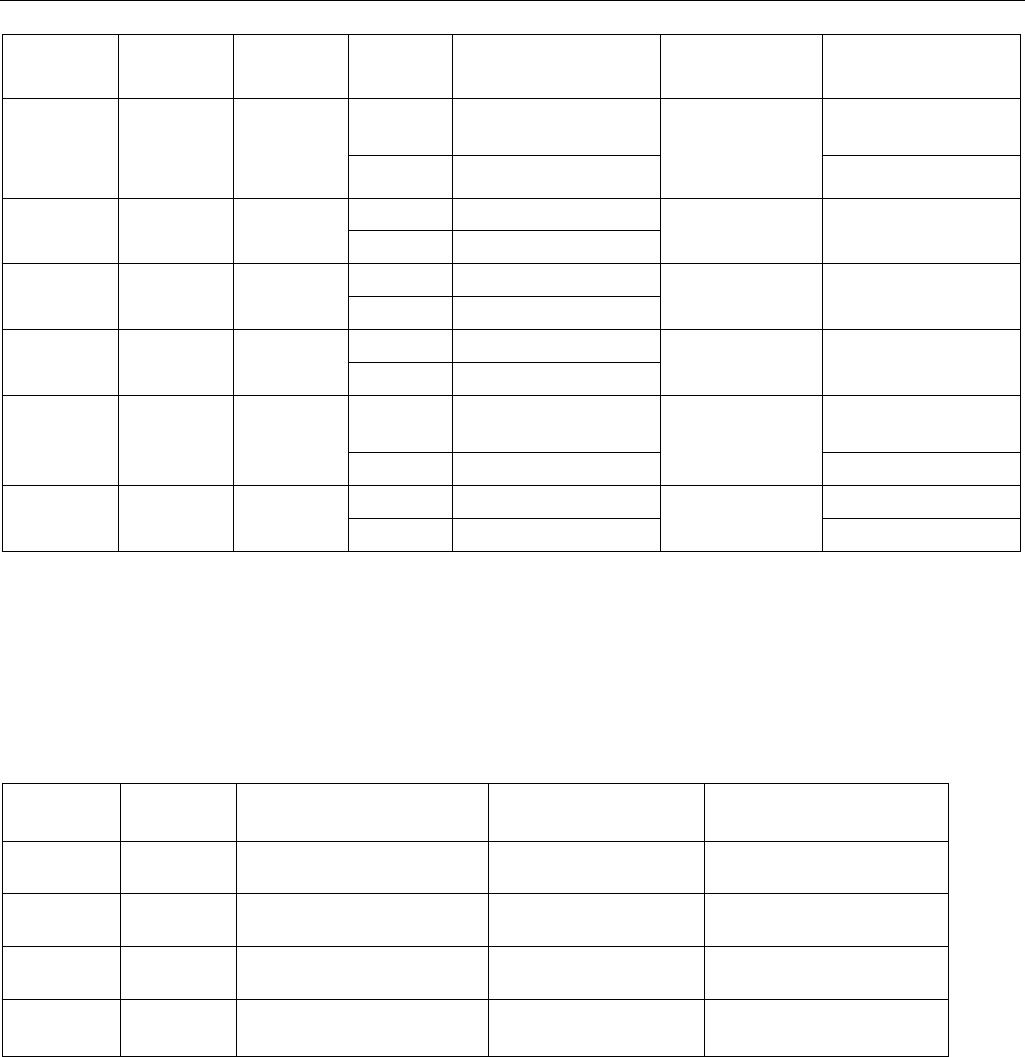
EN0 (bit) (Default EN0 = 1)
If EN0 = 1 and PDN0 = 0, the CTRL0 pin functions as an output enable for OUT0, the frequency of the
output is determined by the SEL0 bit.
If PDN0 = 1, the EN0 bit is ignored, CTRL0 will function as a power-down, output OUT0 will always be
enabled on power-up, and its frequency is determined by the SEL0 bit.
If EN0 = 0, the function of CTRL0 is determined by the SEL0 and PDN0 bits. (See Table 1.)
SEL0 (Default SEL0 = 1)
If SEL0 = 1 and EN0 = PDN0 = 0, the CTRL0 pin determines the state of the MUX, (i.e., the output
frequency of OUT0).
If CTRL0 = 0, the output will be the master clock frequency.
If CTRL0 = 1, the output will be the output frequency of the M prescaler.
If either EN0 or PDN0 = 1, then SEL0 determines the frequency of OUT0 when it is enabled.
If SEL0 = 0, the output will be the master clock frequency.
If SEL0 = 1, the output will be the output frequency of the M prescaler. (See Table 1.)
PDN0 (Default PDN0 = 0)
This bit (if set to 1) causes CTRL0 to perform a power-down function, regardless of the setting of the
other bits.
If PDN0 = 0, the function of CTRL0 is determined by the values of EN0 and SEL0.
NOTE:
When EN0 = SEL0 = PDN0 = 0, CTRL0 also functions as a power-down. This is a special case where all
the OUT0 circuitry is disabled even when the device is powered up. This feature can be used to save
power when OUT0 is not used. (See Table 1.)
PDN1 (Default PDN1 = 0)
If PDN1 = 1, CTRL1 will function as a power-down.
If PDN1 = 0, CTRL1 functions as an output enable for OUT1 only. (See Table 2.)
NOTES (ON OUTPUT ENABLE AND POWER-DOWN):
1. Both enables are “smart” and wait for the output to be low before going to Hi-Z.
2. Power-down sequence first disables both outputs before powering down the device.
3. On power-up, the outputs are disabled until the clock has stabilized (~8000 cycles).
4. The device cannot be programmed in power-down mode.
5. A power-down command must persist for at least 2 cycles of the lowest output frequency plus 10µs.
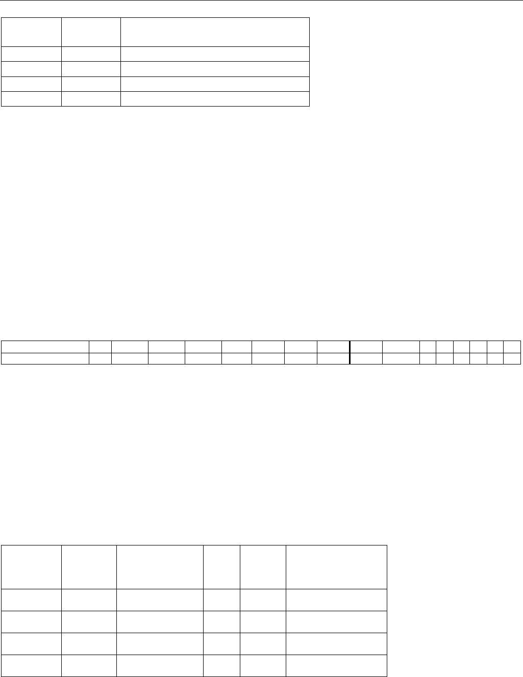
DIV WORD
MSB LSB MSB LSB
N9 N8 N7 N6 N5 N4 N3 N2 N1 N0 X X X X X X
first data byte second data byte
N
These ten bits determine the value of the programmable divider (N). The range of divisor values is from 2
to 1025, and is equal to the programmed value of N plus 2. (See Table 5.)

DS1077LU-40+

Mfr. #:
Manufacturer:
Maxim Integrated
Description:
Clock Generators & Support Products EconOscillator/Dvdr 40Mhz 118mil 2-Wire
Lifecycle:
New from this manufacturer.
Delivery:
DHL FedEx Ups TNT EMS
Payment:
T/T Paypal Visa MoneyGram Western Union