MIC5206-3.0YMM

Micrel, Inc. MIC5206
May 2006
4
M9999-051506
(408) 955-1690
Absolute Maximum Ratings
(1)
Supply Input Voltage (V
IN
).............................. –20V to +20V
Enable Input Voltage (V
EN
)............................. –20V to +20V
Power Dissipation (P
D
) .......................... Internally Limited
(3)
Junction Temperature (T
J
) ........................–40°C to +125°C
Lead Temperature (soldering, 5 sec)......................... 260°C
Operating Ratings
(2)
Supply Input Voltage (V
IN
)............................. +2.5V to +16V
Enable Input Voltage (V
EN
)..................................... 0V to V
IN
Junction Temperature ...............................–40°C to +125°C
SOT-23-5 (θ
JA
)
(3)
MSOP-8 (θ
JA
)
(3)
Electrical Characteristics
V
IN
= V
OUT
+ 1V; I
L
= 100µA; C
L
= 1.0µF; V
EN
2.0V; T
J
= 25°C, bold values indicate –40°C < T
J
< +125°C, unless noted.
Symbol Parameter Condition Min Typ Max Units
V
O
Output Voltage Accuracy Variation from nominal V
OUT
–1
–2
1
2
%
%
V
O
/T
Output Voltage Temperature
Coefficient
Note 4
40
ppm/°C
V
O
/V
O
Line Regulation V
IN
= V
OUT
+ 1V to 16V
V
O
/V
O
Load Regulation
I
L
= 0.1mA to 150mA, Note 5
V
IN
V
O
Dropout Voltage, Note 6 I
L
= 100µA
I
L
= 50mA
I
L
= 100mA
I
L
= 150mA
17
110
140
165
50
70
150
230
250
300
275
350
mV
mV
mV
mV
mV
mV
mV
mV
I
GND
Quiescent Current
V
EN
0.4V (shutdown)
V
EN
0.18V (shutdown)
0.01
1
5
µA
µA
I
GND
Ground Pin Current, Note 7 V
EN
2.0V, I
L
= 100µA
I
L
= 50mA
I
L
= 100mA
I
L
= 150mA
80
350
600
1300
125
150
600
800
1000
1500
1900
2500
µA
µA
µA
µA
µA
µA
µA
µA
PSRR Ripple Rejection 75 dB
I
LIMIT
Current Limit V
OUT
= 0V
320
500 mA
V
O
/P
D
Thermal Regulation
Note 8
0.05 %/W
e
no
Output Noise I
L
= 50mA, C
L
= 4.7µF, 470pF from BYP to
GND (MM package only)
260 nVHz
Enable Input
V
IL
Enable Input Logic-Low Voltage Regulator shutdown
0.4
0.18
V
V
V
IH
Enable Input Logic-High
Voltage
Regulator enable
2.0
V
I
IL
I
IH
Enable Input Current
V
IL
0.4V
V
IL
0.18V
V
IH
2.0V
V
IH
2.0V
0.01
5
–1
–2
20
25
µA
µA
µA
µA
Micrel, Inc. MIC5206
May 2006
5
M9999-051506
(408) 955-1690
Symbol Parameter Condition Min Typ Max Units
Error Flag Output
V
ERR
Flag Threshold
Undervoltage condition (below nominal)
Note 9
–2 –6 –10 %
V
OL
Output Logic-Low Voltage I
L
= 1mA, undervoltage condition 0.2
0.4
V
I
FL
Flag Leakage Current Flag off, V
FLAG
= 0V to 16V –1 0.1 +1 µA
Notes:
1. Exceeding the absolute maximum rating may damage the device.
2. The device is not guaranteed to function outside its operating rating.
3. The maximum allowable power dissipation at any T
A
(ambient temperature) is P
D(max)
= (T
J(max)
–T
A
) / θ
JA
. Exceeding the maximum allowable power
dissipation will result in excessive die temperature, and the regulator will go into thermal shutdown. The θ
JA
of theMIC5205-x.xBM5 (all versions) is
220°C/W, and the MIC5206-x.xBMM (all versions) is 200°C/W, mounted on a PC board (see “Thermal Considerations” for further details).
4. Output voltage temperature coefficient is defined as the worst case voltage change divided by the total temperature range.
5. Regulation is measured at constant junction temperature using low duty cycle pulse testing. Parts are tested for load regulation in the load range
from 0.1mA to 150mA. Changes in output voltage due to heating effects are covered by the thermal regulation specification.
6. Dropout Voltage is defined as the input to output differential at which the output voltage drops 2% below its nominal value measured at 1Vdifferential.
7. Ground pin current is the regulator quiescent current plus pass transistor base current. The total current drawn from the supply is the sum of the load
current plus the ground pin current.
8. Thermal regulation is defined as the change in output voltage at a time “t” after a change in power dissipation is applied, excluding load or line
regulation effects. Specifications are for a 150mA load pulse at V
IN
= 16V for t = 10ms.
9. The error flag comparator includes 3% hysteresis.
Micrel, Inc. MIC5206
May 2006
6
M9999-051506
(408) 955-1690
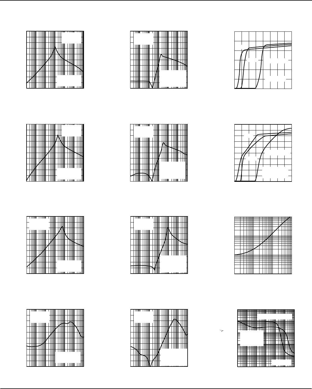
Typical Characteristics
-100
-80
-60
-40
-20
0
1E+1 1E+2 1E+31E+41E+51E+61E+7
)Bd(RRSP
FREQUENCY (Hz)
Power Supply
Rejection Ratio
I
OUT
= 100µA
C
OUT
= 1µF
V
IN
= 6V
V
OUT
= 5V
10
100
1k 10k
100k
1M
10M
-100
-80
-60
-40
-20
0
1E+1 1E+2 1E+3 1E+4 1E+5 1E+6 1E+7
)Bd(RRSP
FREQUENCY (Hz)
Power Supply
Rejection Ratio
I
OUT
= 100µA
C
OUT
= 2.2µF
C
BYP
= 0.01µF
V
IN
= 6V
V
OUT
= 5V
10
100
1k 10k
100k
1M
10M
0
10
20
30
40
50
60
0 0.1 0.2 0.3 0.4
)Bd(NOITCEJERELPPIR
VOLTAGE DROP (V)
Power Supply Ripple Rejection
vs. Voltage Drop
I
OUT
= 100mA
10mA
1mA
C
OUT
= 1µF
-100
-80
-60
-40
-20
0
1E+1 1E+2 1E+3 1E+4 1E+5 1E+61E+7
)Bd(RRSP
FREQUENCY (Hz)
Power Supply
Rejection Ratio
I
OUT
= 1mA
C
OUT
= 1µF
V
IN
= 6V
V
OUT
= 5V
10
100
1k 10k
100k
1M
10M
-100
-80
-60
-40
-20
0
1E+1 1E+2 1E+3 1E+4 1E+5 1E+6 1E+7
)Bd(RRSP
FREQUENCY (Hz)
Power Supply
Rejection Ratio
I
OUT
= 1mA
C
OUT
= 2.2µF
C
BYP
= 0.01µF
V
IN
= 6V
V
OUT
= 5V
10
100
1k 10k
100k
1M
10M
0
10
20
30
40
50
60
70
80
90
100
0 0.1 0.2 0.3 0.4
)Bd(NOITCEJERELPPIR
VOLTAGE DROP (V)
Power Supply Ripple Rejection
vs. Voltage Drop
I
OUT
= 100mA
10mA
1mA
C
OUT
= 2.2µF
C
BYP
= 0.01µF
-100
-80
-60
-40
-20
0
1E+1 1E+2 1E+31E+41E+51E+61E+7
)Bd(RRSP
FREQUENCY (Hz)
Power Supply
Rejection Ratio
I
OUT
= 10mA
C
OUT
= 1µF
V
IN
= 6V
V
OUT
= 5V
10
100
1k 10k
100k
1M
10M
-100
-80
-60
-40
-20
0
1E+1 1E+2 1E+31E+41E+51E+61E+7
)Bd(RRSP
FREQUENCY (Hz)
Power Supply
Rejection Ratio
I
OUT
= 10mA
C
OUT
= 2.2µF
C
BYP
= 0.01µF
V
IN
= 6V
V
OUT
= 5V
10
100
1k 10k
100k
1M
10M
10
100
1000
10000
10 100 1000 10000
(EMI)s
CAPACITANCE (pF)
Turn-On Time
vs. Bypass Capacitance
-100
-80
-60
-40
-20
0
1E+1 1E+2 1E+31E+41E+51E+61E+7
)Bd(RRSP
FREQUENCY (Hz)
Power Supply
Rejection Ratio
I
OUT
= 100mA
C
OUT
= 1µF
V
IN
= 6V
V
OUT
= 5V
10
100
1k 10k
100k
1M
10M
-100
-80
-60
-40
-20
0
1E+1 1E+2 1E+31E+41E+51E+61E+7
)Bd(RRSP
FREQUENCY (Hz)
Power Supply
Rejection Ratio
I
OUT
= 100mA
C
OUT
= 2.2µF
C
BYP
= 0.01µF
V
IN
= 6V
V
OUT
= 5V
10
100
1k 10k
100k
1M
10M
0.0001
0.001
0.01
0.1
1
10
1E+1 1E+2 1E+3 1E+41E+5 1E+61E+
7
(ESIO/V )zH
FREQUENCY (Hz)
Noise Performance
10
100
1k
10k 100k 1M 10M
1mA
C
OUT
= 1µF
C
BYP
= 10nF
10mA, C
OUT
= 1µF
V
OUT
= 5V

MIC5206-3.0YMM

Mfr. #:
Manufacturer:
Microchip Technology / Micrel
Description:
LDO Voltage Regulators 150mA 1% Low Noise LDO w/Flag
Lifecycle:
New from this manufacturer.
Delivery:
DHL FedEx Ups TNT EMS
Payment:
T/T Paypal Visa MoneyGram Western Union