4
0395F–PEEPR–08/09
AT28LV010
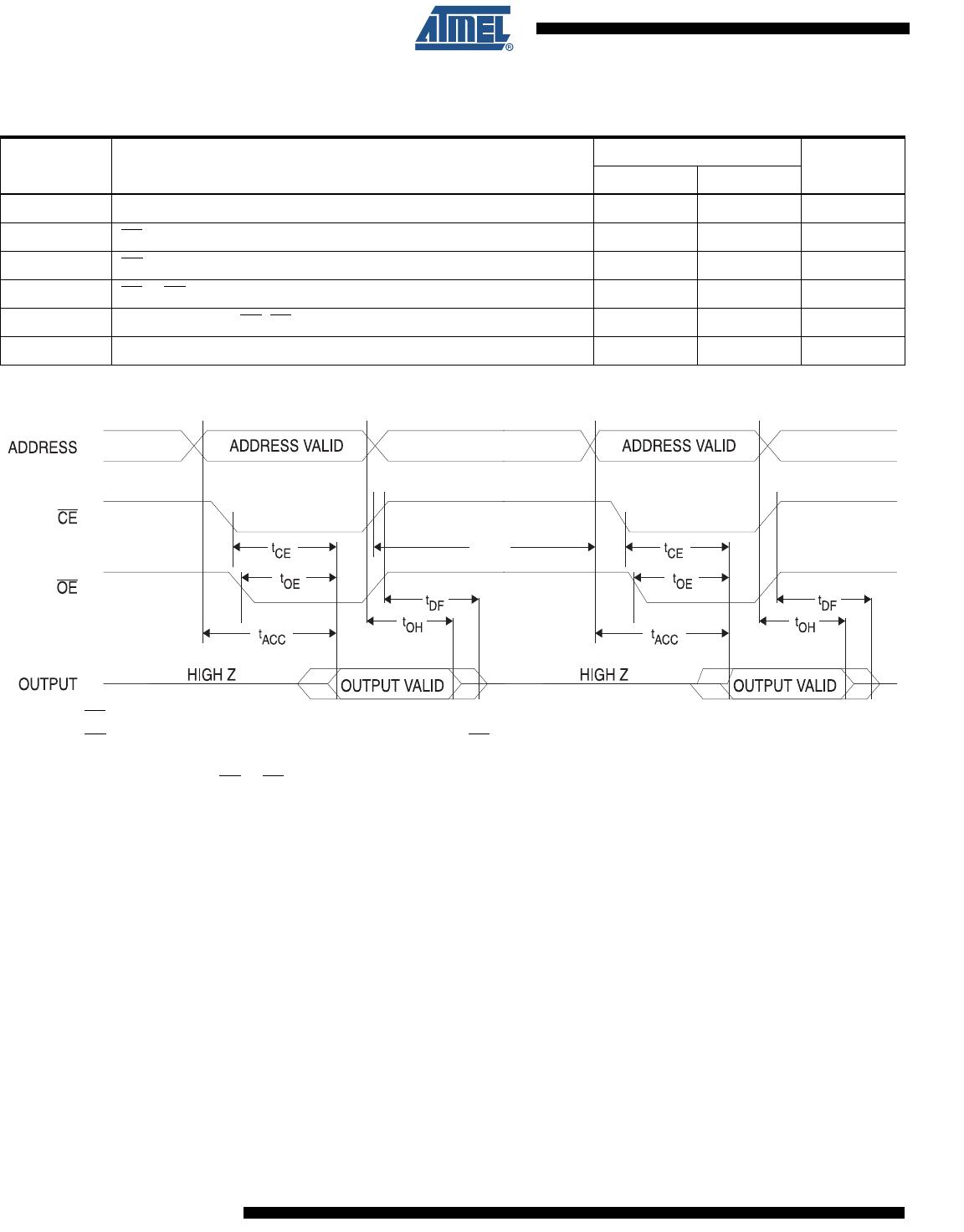
4.3 DATA Polling
The AT28LV010 features DATA Polling to indicate the end of a write cycle. During a byte or
page write cycle an attempted read of the last byte written will result in the complement of the
written data to be presented on I/O7. Once the write cycle has been completed, true data is
valid on all outputs, and the next write cycle may begin. DATA
Polling may begin at anytime
during the write cycle.
4.4 Toggle Bit
In addition to DATA Polling the AT28LV010 provides another method for determining the end
of a write cycle. During the write operation, successive attempts to read data from the device
will result in I/O6 toggling between one and zero. Once the write has completed, I/O6 will stop
toggling and valid data will be read. Reading the toggle bit may begin at any time during the
write cycle.
4.5 Data Protection
If precautions are not taken, inadvertent writes may occur during transitions of the host system
power supply. Atmel
®
has incorporated both hardware and software features that will protect
the memory against inadvertent writes.
4.5.1 Hardware Protection
Hardware features protect against inadvertent writes to the AT28LV010 in the following ways:
(a) V
CC
power-on delay – once V
CC
has reached 2.0V (typical) the device will automatically
time out 5 ms (typical) before allowing a write; (b) write inhibit – holding any one of OE
low, CE
high or WE high inhibits write cycles; and (c) noise filter – pulses of less than 15 ns (typical) on
the WE
or CE inputs will not initiate a write cycle.
4.5.2 Software Data Protection
The AT28LV010 incorporates the industry standard software data protection (SDP) function.
Unlike standard 5-volt only EEPROM’s, the AT28LV010 has SDP enabled at all times. There-
fore, all write operations must be preceded by the SDP command sequence.
The data in the 3-byte command sequence is not written to the device; the addresses in the
command sequence can be utilized just like any other location in the device. Any attempt to
write to the device without the 3-byte sequence will start the internal timers. No data will be
written to the device. However, for the duration of t
WC
, read operations will effectively be poll-
ing operations.