ADF4106 Data Sheet
Parameter B Version
1
B Chips
2
(typ) Unit Test Conditions/Comments
NOISE CHARACTERISTICS
Normalized Phase Noise Floor
(PN
SYNTH
)
11
–223 –223 dBc/Hz typ
PLL loop B/W = 500 kHz, measured at 100 kHz
offset
Normalized 1/f Noise (PN
1_f
)
12
−122 −122 dBc/Hz typ 10 kHz offset; normalized to 1 GHz
Phase Noise Performance
13
@ VCO output
900 MHz
14
–92.5 −92.5 dBc/Hz typ @ 1 kHz offset and 200 kHz PFD frequency
5800 MHz
15
−76.5 −76.5 dBc/Hz typ @ 1 kHz offset and 200 kHz PFD frequency
5800 MHz
16
−83.5 −83.5 dBc/Hz typ @ 1 kHz offset and 1 MHz PFD frequency
Spurious Signals
900 MHz
14
–90/–92 –90/–92 dBc typ @ 200 kHz/400 kHz and 200 kHz PFD frequency
@ 200 kHz/400 kHz and 200 kHz PFD frequency
5800 MHz
16
–70/–75 –70/–75 dBc typ @ 1 MHz/2 MHz and 1 MHz PFD frequency
1
Operating temperature range (B Version) is –40°C to +85°C.
2
The B chip specifications are given as typical values.
3
This is the maximum operating frequency of the CMOS counters. The prescaler value should be chosen to ensure that the RF input is divided down to a frequency that
is less than this value.
4
AV
DD
= DV
DD
= 3 V.
5
AC coupling ensures AV
DD
/2 bias.
6
Guaranteed by design. Sample tested to ensure compliance.
7
T
A
= 25°C; AV
DD
= DV
DD
= 3 V; P = 16; RF
IN
= 900 MHz.
8
T
A
= 25°C; AV
DD
= DV
DD
= 3 V; P = 16; RF
IN
= 2.0 GHz.
9
T
A
= 25°C; AV
DD
= DV
DD
= 3 V; P = 32; RF
IN
= 6.0 GHz.
10
T
A
= 25°C; AV
DD
= DV
DD
= 3.3 V; R = 16383; A = 63; B = 891; P = 32; RF
IN
= 6.0 GHz.
11
The synthesizer phase noise floor is estimated by measuring the in-band phase noise at the output of the VCO and subtracting 20 log N (where N is the N divider
value) and 10 log F
PFD
. PN
SYNTH
= PN
TOT
− 10 log F
PFD
− 20 log N.
12
The PLL phase noise is composed of 1/f (flicker) noise plus the normalized PLL noise floor. The formula for calculating the 1/f noise contribution at an RF frequency, f
RF
,
and at a frequency offset, f, is given by PN = PN
1_f
+ 10 log(10 kHz/f) + 20 log(f
RF
/1 GHz). Both the normalized phase noise floor and flicker noise are modeled in
ADIsimPLL.
13
The phase noise is measured with the EV-ADF4106SD1Z evaluation board and the Agilent E4440A Spectrum Analyzer. The spectrum analyzer provides the REFIN for
the synthesizer (f
REFOUT
= 10 MHz @ 0 dBm).
14
f
REFIN
= 10 MHz; f
PFD
= 200 kHz; Offset Frequency = 1 kHz; f
RF
= 900 MHz; N = 4500; Loop B/W = 20 kHz.
15
f
REFIN
= 10 MHz; f
PFD
= 200 kHz; Offset Frequency = 1 kHz; f
RF
= 5800 MHz; N = 29000; Loop B/W = 20 kHz.
16
f
REFIN
= 10 MHz; f
PFD
= 1 MHz; Offset Frequency = 1 kHz; f
RF
= 5800 MHz; N = 5800; Loop B/W = 100 kHz.
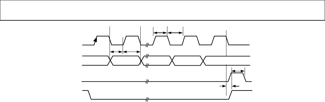
TIMING CHARACTERISITICS
AV
DD
= DV
DD
= 3 V ± 10%, AV
DD
≤ V
P
≤ 5.5 V, AGND = DGND = CPGND = 0 V, R
SET
= 5.1 kΩ, dBm referred to 50 Ω, T
A
= T
MAX
to T
MIN
,
unless otherwise noted.
Table 2.
Parameter Limit
1
(B Version) Unit Test Conditions/Comments
t
1
10 ns min DATA to CLOCK Setup Time
t
2
10 ns min DATA to CLOCK Hold Time
t
3
25 ns min CLOCK High Duration
t
4
25 ns min CLOCK Low Duration
t
5
10 ns min CLOCK to LE Setup Time
t
6
20 ns min LE Pulse Width
1
Operating temperature range (B Version) is –40°C to +85°C.
Rev. F | Page 4 of 24