AD632 Data Sheet
Rev. D | Page 6 of 12
PIN CONFIGURATIONS AND FUNCTION DESCRIPTIONS
Figure 2. Pin Configuration, H-Package, TO-100
Figure 3. Pin Configuration, D-Package, SBDIP
Table 3. Pin Function Descriptions, 10-Pin TO-100
Pin No. Mnemonic Description
1 Y1 Y Multiplicand Noninverting Input.
2 +V
S
Positive Supply Voltage.
3 Z1 Summing Node Noninverting Input.
4 OUT Product.
5 −V
S
Negative Supply Voltage.
6 X1 X Multiplicand Noninverting Input.
7 X2 X Multiplicand Inverting Input.
8 Z2 Summing Node Inverting Input.
9 V
OS
Offset Voltage Adjustment.
10 Y2 Y Multiplicand Inverting Input.
Table 4. Pin Function Descriptions, 14-Lead SBDIP
Pin No. Mnemonic Description
1 Z1 Summing Node Noninverting Input.
2 OUT Product.
3 −V
S
Negative Supply Voltage.
4, 5, 6, 8 NC
No Connection. Do not connect to
this pin.
7 X1 X Multiplicand Noninverting Input.
9 X2 X Multiplicand Noninverting Input.
10 Z2 Summing Node Inverting Input.
11 V
OS
Offset Voltage Adjustment.
12 Y2 Y Multiplicand Inverting Input.
13 Y1 Y Multiplicand Noninverting Input.
14 +V
S
Positive Supply Voltage.
V
OS
Z2 (GND)
Y2
–V
S
Z1
OUT
+V
S
Y1
X2
X1
6
7
8
9
10
3
4
2
1
5
(Not to Scale)
AD632
09040-001
1
2
3
4
+V
S
14
Y1
13
Y2
12
V
OS
11
5
Z2
10
6
X2
9
Z1
OUT
–V
S
NC
NC
NC
X1
7
NC
8
NC = NO CONNECT
AD632
TOP VIEW
(Not to Scale)
09040-002
Data Sheet AD632
Rev. D | Page 7 of 12
TYPICAL PERFORMANCE CHARACTERISTICS
Typical @ 25°C with ±V
S
= 15 V.
Figure 4. AC Feedthrough vs. Frequency
Figure 5. Frequency Response as a Multiplier
Figure 6. Frequency Response vs. Divider Denominator Input Voltage
1000
0.1
10 10M
09040-004
FEEDTHROUGH (mV p-p)
FREQUENCY (Hz)
100 1k
10k 100k 1M
100
10
1
Y FEEDTHROUGH
X FEEDTHROUGH
–30
10k 10M
09040-005
OUTPUT RESPONSE (dB)
FREQUENCY (Hz)
100k 1M
0
–10
–20
C
L
= 0pF
C
L
= 1000pF
NORMAL
CONNECTION
C
L
≤ 1000pF
C
F
≤ 200pF
WITH ×10
FEEDBACK
ATTENUATOR
C
L
≤ 1000pF
C
F
= 0pF
0dB = 0.1V rms, R
L
= 2kΩ
40
20
0
V
O
V
z
–20
1k 10M
09040-006
OUTPUT (dB )
FREQUENCY (Hz)
10k 100k 1M
V
X
= 100mV DC
V
Z
= 10mV rms
V
X
= 1V DC
V
Z
= 100mV rms
V
X
= 10V DC
V
Z
= 1V rms
0dB = 1V rms, R
L
= 2kΩ
AD632 Data Sheet
Rev. D | Page 8 of 12
OPERATION AS A MULTIPLIER
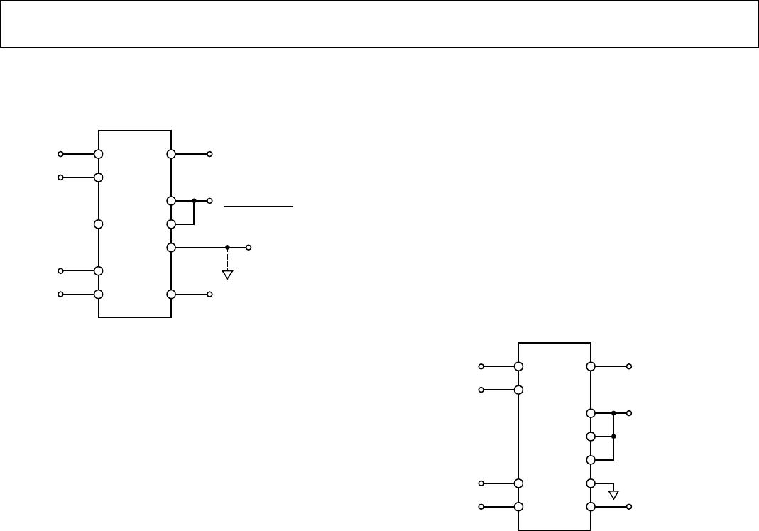
Figure 7 shows the basic connection for multiplication. Note
that the circuit meets all specifications without trimming.
Figure 7. Basic Multiplier Connection
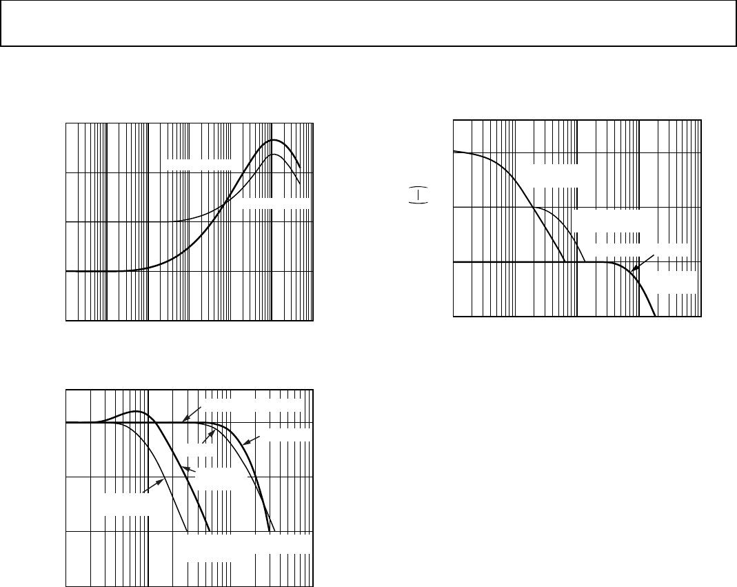
When needed, the user can reduce ac feedthrough to a minimum
(as in a suppressed carrier modulator) by applying an external
trim voltage (±30 mV range required) to the X or Y input. Figure 4
shows the typical ac feedthrough with this adjustment mode.
Note that the feedthrough of the Y input is a factor of 10 lower
than that of the X input and is to be used for applications where
null suppression is critical.
The Z
2
terminal of the AD632 can be used to sum an additional
signal into the output. In this mode, the output amplifier behaves
as a voltage follower with a 1 MHz small signal bandwidth and
a 20 V/μs slew rate. Always reference this terminal to the ground
point of the driven system, particularly if this is remote. Like-
wise, reference the differential inputs to their respective signal
common potentials to realize the full accuracy of the AD632.
A much lower scaling voltage can be achieved without any reduc-
tion of input signal range using a feedback attenuator, as shown
in Figure 8. In this example, the scale is such that V
OUT
= XY, so
that the circuit can exhibit a maximum gain of 10. This connection
results in a reduction of bandwidth to about 80 kHz without the
peaking capacitor, C
F
. In addition, the output offset voltage is
increased by a factor of 10 making external adjustments necessary
in some applications.
Feedback attenuation also retains the capability for adding a
signal to the output. Signals can be applied to the Z terminal,
where they are amplified by −10, or to the common ground
connection where they are amplified by −1. Input signals can
also be applied to the lower end of the 2.7 kΩ resistor, giving a
gain of +9.
Figure 8. Connections for Scale Factor of Unity
X
1
+V
S
X
2
V
OS
OUT
Z
1
Z
2
Y
1
Y
2
–V
S
–15V
+15V
X INPUT
±10V FS
±12V PK
Y INPUT
±10V FS
±12V PK
OUTPUT, ±12V PK
(X
1
– X
2
) (Y
1
– Y
2
)
OPTIONAL SUMMIN
G
INPUT, Z, ±10V PK;
V
OS
TERMINAL
NOT USED
10
+ Z
2
=
09040-008
X
1
+V
S
X
2
OUT
Z
1
Z
2
V
OS
Y
1
Y
2
–V
S
–15V
+15V
X INPUT
±10V FS
±12V PK
Y INPUT
±10V FS
±12V PK
OUTPUT, ±12V PK
= (X
1
– X
2
) (Y
1
– Y
2
)
(SCALE = 1)
09040-009

AD632BHZ

Mfr. #:
Manufacturer:
Analog Devices Inc.
Description:
Multipliers / Dividers Internally Trimmed Prec IC Mult
Lifecycle:
New from this manufacturer.
Delivery:
DHL FedEx Ups TNT EMS
Payment:
T/T Paypal Visa MoneyGram Western Union