HEF4060B All information provided in this document is subject to legal disclaimers. © NXP B.V. 2011. All rights reserved.
Product data sheet Rev. 7 — 16 November 2011 4 of 15
NXP Semiconductors
HEF4060B
14-stage ripple-carry binary counter/divider and oscillator
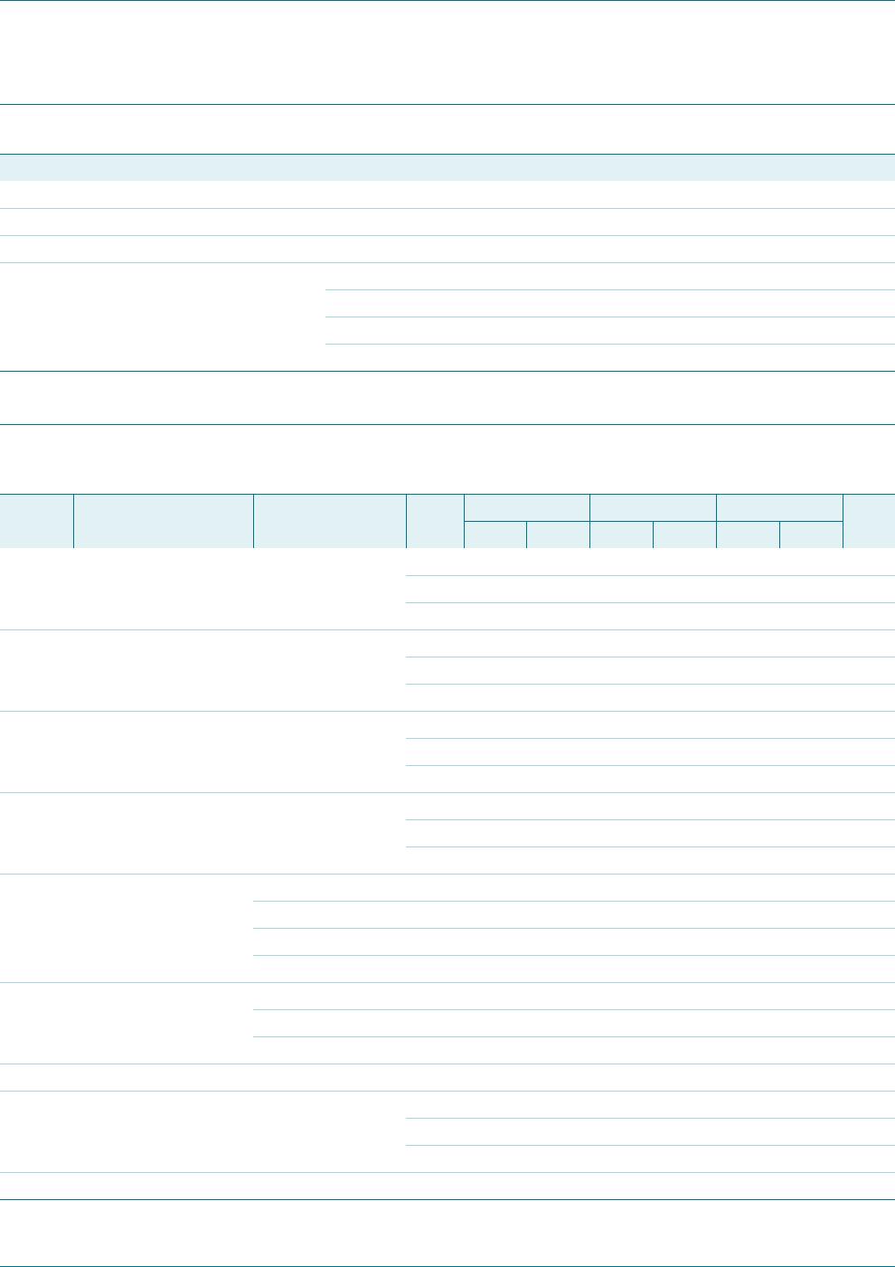
8. Recommended operating conditions
9. Static characteristics
Table 5. Recommended operating conditions
Symbol Parameter Conditions Min Typ Max Unit
V
DD
supply voltage 3 - 15 V
V
I
input voltage 0 - V
DD
V
T
amb
ambient temperature in free air 40 - +85 C
t/V input transition rise and fall
rate
input MR
V
DD
= 5 V - - 3.75 s/V
V
DD
= 10 V - - 0.5 s/V
V
DD
= 15 V - - 0.08 s/V
Table 6. Static characteristics
V
SS
= 0 V; V
I
= V
SS
or V
DD
unless otherwise specified.
Symbol Parameter Conditions V
DD
T
amb
= 40 C T
amb
= 25 C T
amb
= 85 C Unit
Min Max Min Max Min Max
V
IH
HIGH-level
input voltage
I
O
< 1 A 5 V 3.5 - 3.5 - 3.5 - V
10 V 7.0 - 7.0 - 7.0 - V
15 V 11.0 - 11.0 - 11.0 - V
V
IL
LOW-level
input voltage
I
O
< 1 A 5 V-1.5-1.5-1.5V
10 V - 3.0 - 3.0 - 3.0 V
15 V - 4.0 - 4.0 - 4.0 V
V
OH
HIGH-level
output voltage
I
O
< 1 A 5 V 4.95 - 4.95 - 4.95 - V
10 V 9.95 - 9.95 - 9.95 - V
15 V 14.95 - 14.95 - 14.95 - V
V
OL
LOW-level
output voltage
I
O
< 1 A 5 V - 0.05 - 0.05 - 0.05 V
10 V - 0.05 - 0.05 - 0.05 V
15 V - 0.05 - 0.05 - 0.05 V
I
OH
HIGH-level
output current
V
O
= 2.5 V 5 V - 1.7 - 1.4 - 1.1 mA
V
O
= 4.6 V 5 V - 0.52 - 0.44 - 0.36 mA
V
O
= 9.5 V 10 V - 1.3 - 1.1 - 0.9 mA
V
O
= 13.5 V 15 V - 3.6 - 3.0 - 2.4 mA
I
OL
LOW-level
output current
V
O
= 0.4 V 5 V 0.52 - 0.44 - 0.36 - mA
V
O
= 0.5 V 10 V 1.3 - 1.1 - 0.9 - mA
V
O
= 1.5 V 15 V 3.6 - 3.0 - 2.4 - mA
I
I
input leakage current 15 V - 0.3 - 0.3 - 1.0 A
I
DD
supply current I
O
= 0 A 5 V - 20 - 20 - 150 A
10 V - 40 - 40 - 300 A
15 V - 80 - 80 - 600 A
C
I
input capacitance - - - - 7.5 - - pF
HEF4060B All information provided in this document is subject to legal disclaimers. © NXP B.V. 2011. All rights reserved.
Product data sheet Rev. 7 — 16 November 2011 5 of 15
NXP Semiconductors
HEF4060B
14-stage ripple-carry binary counter/divider and oscillator
10. Dynamic characteristics
[1] The typical values of the propagation delay and transition times are calculated from the extrapolation formulas shown (C
L
in pF).
[2] t
pd
is the same as t
PHL
and t
PLH
.
[3] t
t
is the same as t
THL
and t
TLH
.
Table 7. Dynamic characteristics
T
amb
= 25
C; V
SS
= 0 V; C
L
= 50 pF; t
r
= t
f
20 ns; unless otherwise specified.
Symbol Parameter Conditions V
DD
Extrapolation formula
[1]
Min Typ Max Unit
t
pd
propagation delay RS Q3;
see Figure 4
5 V
[2]
183 ns + (0.55 ns/pF) C
L
- 210 420 ns
10 V 69 ns + (0.23 ns/pF) C
L
-80160ns
15 V 42 ns + (0.16 ns/pF) C
L
-50100ns
Qn Qn + 1;
see Figure 4
5 V - - 25 50 ns
10 V - - 10 20 ns
15 V - - 6 12 ns
MR Qn;
HIGH to LOW
see Figure 4
5 V 73 ns + (0.55 ns/pF) C
L
- 100 200 ns
10 V 29 ns + (0.23 ns/pF) C
L
-4080ns
15 V 22 ns + (0.16 ns/pF) C
L
-3060ns
t
t
transition time see Figure 4 5 V
[3]
10 ns + (1.00 ns/pF) C
L
-60120ns
10 V 9 ns + (0.42 ns/pF) C
L
-3060ns
15 V 6 ns + (0.28 ns/pF) C
L
-2040ns
t
W
pulse width minimum width;
RS HIGH;
see Figure 4
5 V 120 60 - ns
10 V 50 25 - ns
15 V 30 15 - ns
minimum width;
MR HIGH;
see Figure 4
5 V 50 25 - ns
10 V 30 15 - ns
15 V 20 10 - ns
t
rec
recovery time input MR;
see Figure 4
5 V 160 80 - ns
10 V 80 40 - ns
15 V 60 30 - ns
f
max
maximum frequency input RS;
see Figure 4
5 V 4 8 - MHz
10 V 10 20 - MHz
15 V 15 30 - MHz
HEF4060B All information provided in this document is subject to legal disclaimers. © NXP B.V. 2011. All rights reserved.
Product data sheet Rev. 7 — 16 November 2011 6 of 15
NXP Semiconductors
HEF4060B
14-stage ripple-carry binary counter/divider and oscillator
[1] Where:
f
i
= input frequency in MHz; f
o
= output frequency in MHz;
C
L
= output load capacitance in pF;
V
DD
= supply voltage in V;
(f
o
C
L
) = sum of the outputs;
C
t
= timing capacitance (pF);
f
osc
= oscillator frequency (MHz).
11. Waveforms
Table 8. Power dissipation
Dynamic power dissipation P
D
and total power dissipation P
tot
can be calculated from the formulas shown. T
amb
= 25
C.
Symbol Parameter Conditions V
DD
Typical formula for P
D
and P
tot
(W)
[1]
P
D
dynamic power
dissipation
per device 5 V P
D
= 700 f
i
+ (f
o
C
L
) V
DD
2
10 V P
D
= 3300 f
i
+ (f
o
C
L
) V
DD
2
15 V P
D
= 8900 f
i
+ (f
o
C
L
) V
DD
2
P
tot
total power
dissipation
when using
the on-chip
oscillator
5V P
tot
= 700 f
osc
+ (f
o
C
L
) V
DD
2
+ 2 C
t
V
DD
2
f
osc
+ 690 V
DD
10 V P
tot
= 3300 f
osc
+ (f
o
C
L
) V
DD
2
+ 2 C
t
V
DD
2
f
osc
+ 6900 V
DD
15 V P
tot
= 8900 f
osc
+ (f
o
C
L
) V
DD
2
+ 2 C
t
V
DD
2
f
osc
+ 22000 V
DD
Measurement points are given in Table 9.
Fig 4. Waveforms showing propagation delays for MR to Qn and CP to Q0, minimum MR, and CP pulse widths
001aaj472
MR input
RS input
Qn output
t
W
t
PHL
t
rec
V
M
t
PLH
t
W
t
PHL
t
t
t
t
1/f
max
V
M
V
M
t
f
t
r
10 %
90 %
10 %
90 %
Table 9. Measurement points
Supply voltage Input Output
V
DD
V
M
V
M
5 V to 15 V 0.5V
DD
0.5V
DD

HEF4060BP,652

Mfr. #:
Manufacturer:
NXP Semiconductors
Description:
Counter ICs 14-STG RC BIN CTR/DIV W/OSC.
Lifecycle:
New from this manufacturer.
Delivery:
DHL FedEx Ups TNT EMS
Payment:
T/T Paypal Visa MoneyGram Western Union

Products related to this Datasheet