HEF4060B All information provided in this document is subject to legal disclaimers. © NXP B.V. 2011. All rights reserved.
Product data sheet Rev. 7 — 16 November 2011 7 of 15
NXP Semiconductors
HEF4060B
14-stage ripple-carry binary counter/divider and oscillator
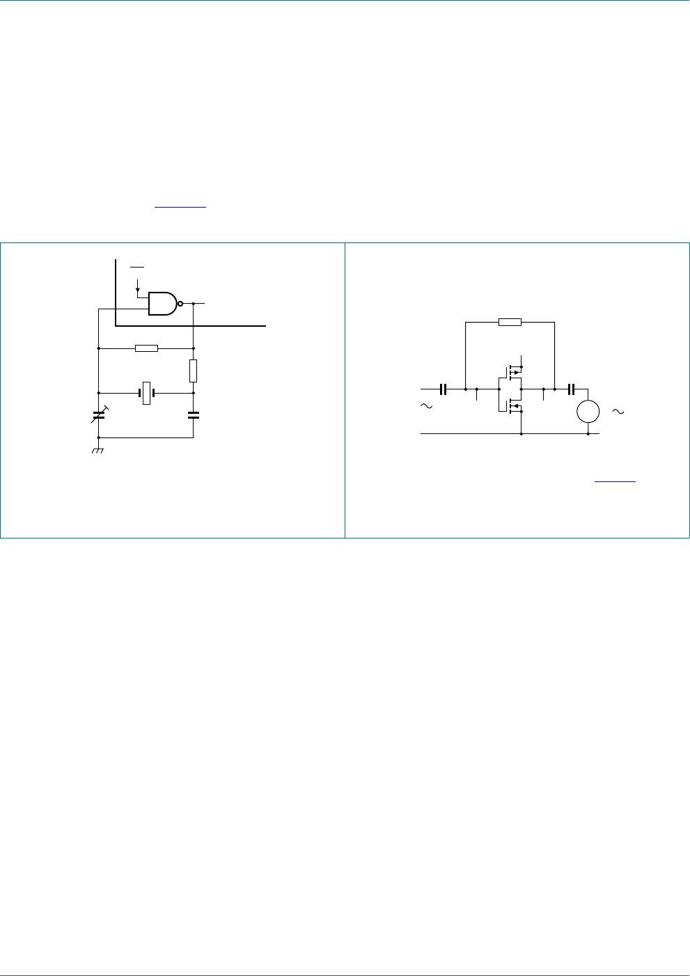
12. RC oscillator
12.1 Timing component limitations
The oscillator frequency is mainly determined by R
t
C
t
, provided R
t
<< R2 and
R2 C2 << R
t
C
t
. The influence of the forward voltage across the input protection
diodes on the frequency is minimized by R2. The stray capacitance C2 should be kept as
small as possible. In consideration of accuracy, C
t
must be larger than the inherent stray
capacitance. R
t
must be larger than the LOCMOS (Local Oxidation Complementary
Metal-Oxide Semiconductor) ‘ON’ resistance in series with it, which typically is 500 at
V
DD
= 5 V, 300 at V
DD
= 10 V and 200 at V
DD
=15V.
Test data is given in Table 10.
Definitions for test circuit:
DUT = Device Under Test;
C
L
= load capacitance including jig and probe capacitance;
R
T
= termination resistance should be equal to the output impedance Z
o
of the pulse generator.
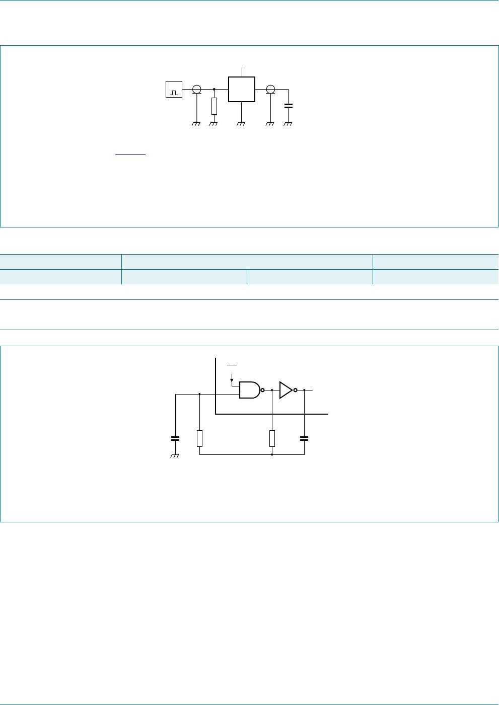
Fig 5. Test circuit for switching times
V
DD
V
I
V
O
001aag182
DUT
C
L
R
T
G
Table 10. Measurement point and test data
Supply voltage Input Load
V
DD
V
I
t
r
, t
f
C
L
5 V to 15 V V
SS
or V
DD
20 ns 50 pF
Typical formula for oscillator frequency:
Fig 6. External component connection for RC oscillator
001aae655
R2 R
t
C
t
C2
RS
MR (from logic)
REXT CEXT
10 9
11
HEF4060B
f
osc
1
2.3 R
t
C
t
------------------------------
=