6.42
IDT70V05S/L
High-Speed 3.3V 8K x 8 Dual-Port Static RAM Industrial and Commercial Temperature Ranges
13
NOTES:
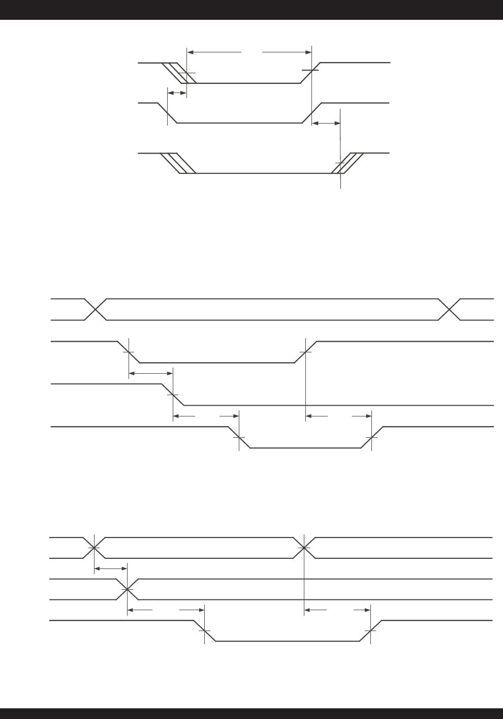
1. Port-to-port delay through SRAM cells from writing port to reading port, refer to “Timing Waveform of Read With BUSY (M/S = V
IH)” or “Timing Waveform of Write With Port-
To-Port Delay (M/S = V
IL)”.
2. To ensure that the earlier of the two ports wins.
3. t
BDD is a calculated parameter and is the greater of 0, tWDD – tWP (actual) or tDDD – tDW (actual).
4. To ensure that the write cycle is inhibited during contention.
5. To ensure that a write cycle is completed after contention.
6. 'X' is part number indicates power rating (S or L).
AC Electrical Characteristics Over the
Operating Temperature and Supply Voltage Range
(6)
51X50V07
ynOl'moC
02X50V07
l'moC
dnI&
52X50V07
ylnOl'moC
lobmySretemaraP.niM.xaM.niM.xaM.niM.xaMtinU
YSUB /M(GNIMIT S V=
HI
)
t
AAB
YSUB hctaMsserddAmorfemiTsseccA
____
51
____
02
____
02sn
t
ADB
YSUB dehctaMtoNsserddAmorfemiTelbasiD
____
51
____
02
____
02sn
t
CAB
YSUB WOLelbanEpihCmorfemiTsseccA
____
51
____
02
____
02sn
t
CDB
YSUB HGIHelbanEpihCmorfemiTelbasiD
____
51
____
71
____
71sn
t
SPA
emiTpu-teSytiroirPnoitartibrA
)2(
5
____
5
____
5
____
sn
t
DDB
YSUB ataDdilaVotelbasiD
)3(
____
81
____
03
____
03sn
t
HW
retfAdloHetirW YSUB
)5(
21
____
51
____
71
____
sn
YSUB /M(GNIMIT S V=
LI
)
t
BW
YSUB etirWottupnI
)4(
0
____
0
____
0
____
sn
t
HW
retfAdloHetirW YSUB
)5(
21
____
51
____
71
____
sn
GNIMITYALEDTROP-OT-TROP
t
DDW
yaleDataDotesluPetirW
)1(
____
03
____
54
____
05sn
t
DDD
yaleDataDdaeRotdilaVataDetirW
)1(
____
52
____
53
____
53sn
a31lbt1492
53X50V07
ylnOl'moC
55X50V07
ylnOl'moC
lobmySretemaraP.niM.xaM.niM.xaMtinU
YSUB /M(GNIMIT S V=
HI
)
t
AAB
YSUB hctaMsserddAmorfemiTsseccA
____
02
____
54sn
t
ADB
YSUB dehctaMtoNsserddAmorfemiTelbasiD
____
02
____
04sn
t
CAB
YSUB WOLelbanEpihCmorfemiTsseccA
____
02
____
04sn
t
CDB
YSUB HGIHelbanEpihCmorfemiTelbasiD
____
02
____
53sn
t
SPA
emiTpu-teSytiroirPnoitartibrA
)2(
5
____
5
____
sn
t
DDB
YSUB ataDdilaVotelbasiD
)3(
____
53
____
04sn
t
HW
retfAdloHetirW YSUB
)5(
52
____
52
____
sn
YSUB /M(GNIMIT S V=
LI
)
t
BW
YSUB etirWottupnI
)4(
0
____
0
____
sn
t
HW
retfAdloHetirW YSUB
)5(
52
____
52
____
sn
GNIMITYALEDTROP-OT-TROP
t
DDW
yaleDataDotesluPetirW
)1(
____
06
____
08sn
t
DDD
yaleDataDdaeRotdilaVataDetirW
)1(
____
54
____
56sn
b31lbt1492