Si8809EDB
www.vishay.com
Vishay Siliconix
S15-0346-Rev. C, 23-Feb-15
1
Document Number: 63301
For technical questions, contact: pmostechsupport@vishay.com
THIS DOCUMENT IS SUBJECT TO CHANGE WITHOUT NOTICE. THE PRODUCTS DESCRIBED HEREIN AND THIS DOCUMENT
ARE SUBJECT TO SPECIFIC DISCLAIMERS, SET FORTH AT www.vishay.com/doc?91000
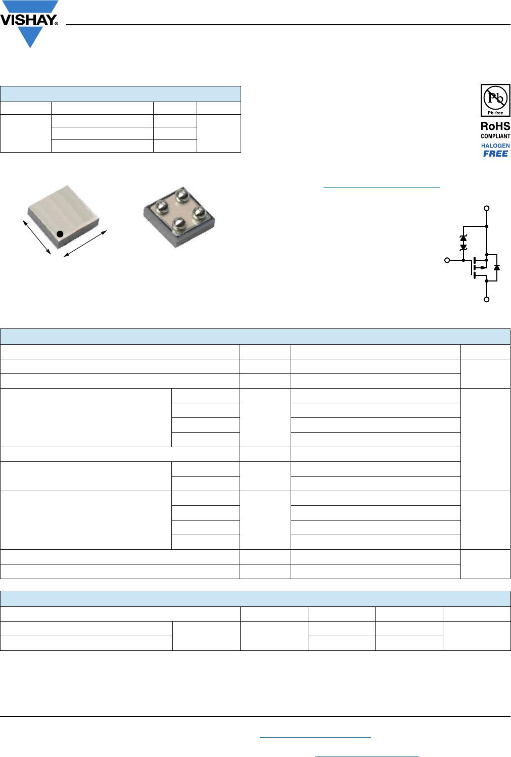
P-Channel 20 V (D-S) MOSFET
Marking Code: xx = AE
xxx = Date/Lot traceability code
Ordering Information:
Si8809EDB-T2-E1 (lead (Pb)-free and halogen-free)
FEATURES
• TrenchFET
®
power MOSFET
• Ultra small 0.8 mm x 0.8 mm outline
• Ultra thin 0.357 mm height
• Typical ESD protection 1000 V HBM
• High speed switching
• Material categorization: for definitions of compliance
please see www.vishay.com/doc?99912
APPLICATIONS
• Portable devices such as cell phones,
smart phones, tablet PCs and media
players
- Load switch
- Battery switch
Notes
a. Surface mounted on 1" x 1" FR4 board with full copper, t = 5 s.
b. Surface mounted on 1" x 1" FR4 board with minimum copper, t = 5 s.
c. Refer to IPC/JEDEC
®
(J-STD-020), no manual or hand soldering.
d. Maximum under steady state conditions is 185 °C/W.
e. Maximum under steady state conditions is 330 °C/W.
PRODUCT SUMMARY
V
DS
(V) R
DS(on)
(Ω)I
D
(A)
a
Q
g
(TYP.)
-20
0.090 at V
GS
= -4.5 V -2.6
6 nC0.119 at V
GS
= -2.5 V -2.3
0.155 at V
GS
= -1.8 V -2
MICRO FOOT
®
0.8 x 0.8
Backside View
1
0.8 mm
0.8 mm
xxx
xx
Bump Side View
1
G
4
D
S
3
S
2
ABSOLUTE MAXIMUM RATINGS (T
A
= 25 °C, unless otherwise noted)
PARAMETER SYMBOL LIMIT UNIT
Drain-Source Voltage V
DS
-20
V
Gate-Source Voltage V
GS
± 8
Continuous Drain Current (T
J
= 150 °C)
T
A
= 25 °C
I
D
-2.6
a
A
T
A
= 70 °C -2.1
a
T
A
= 25 °C -1.9
b
T
A
= 70 °C -1.5
b
Pulsed Drain Current (t = 300 μs) I
DM
-13
Continuous Source-Drain Diode Current
T
A
= 25 °C
I
S
-0.7
a
T
A
= 25 °C -0.4
b
Maximum Power Dissipation
T
A
= 25 °C
P
D
0.9
a
W
T
A
= 70 °C 0.6
a
T
A
= 25 °C 0.5
b
T
A
= 70 °C 0.3
b
Operating Junction and Storage Temperature Range T
J
, T
stg
-55 to +150
°C
Soldering Recommendations (Peak Temperature)
c
260
THERMAL RESISTANCE RATINGS
PARAMETER SYMBOL TYPICAL MAXIMUM UNIT
Maximum Junction-to-Ambient
a, d
t ≤ 5 s R
thJA
105 135
°C/W
Maximum Junction-to-Ambient
b, e
200 260