Si8809EDB
www.vishay.com
Vishay Siliconix
S15-0346-Rev. C, 23-Feb-15
5
Document Number: 63301
For technical questions, contact: pmostechsupport@vishay.com
THIS DOCUMENT IS SUBJECT TO CHANGE WITHOUT NOTICE. THE PRODUCTS DESCRIBED HEREIN AND THIS DOCUMENT
ARE SUBJECT TO SPECIFIC DISCLAIMERS, SET FORTH AT www.vishay.com/doc?91000
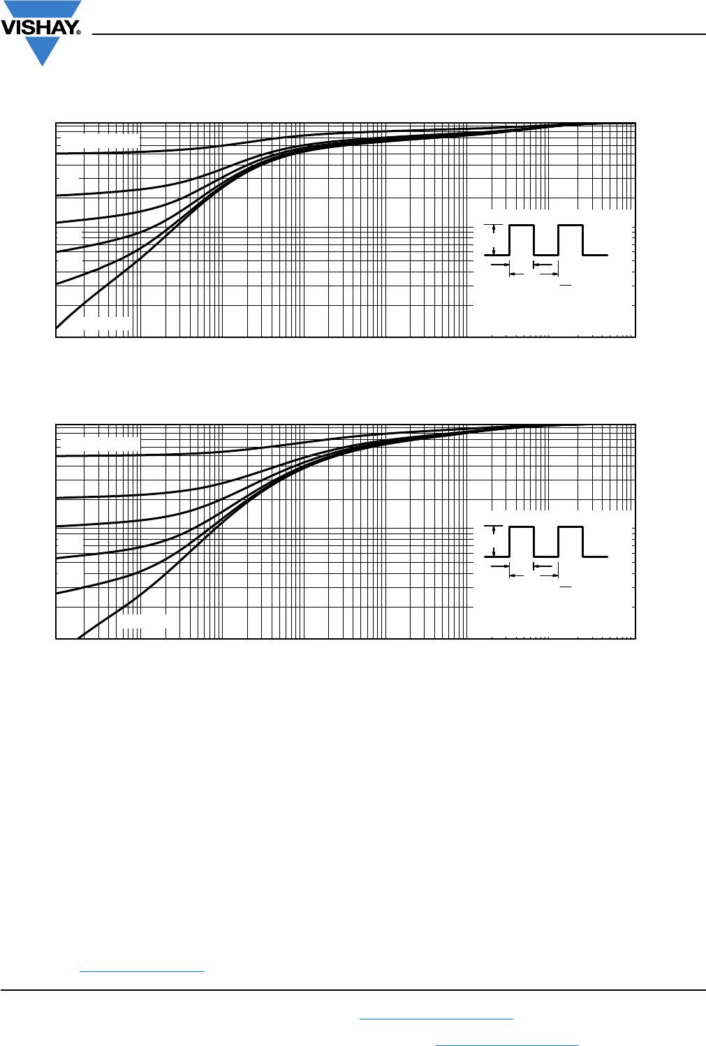
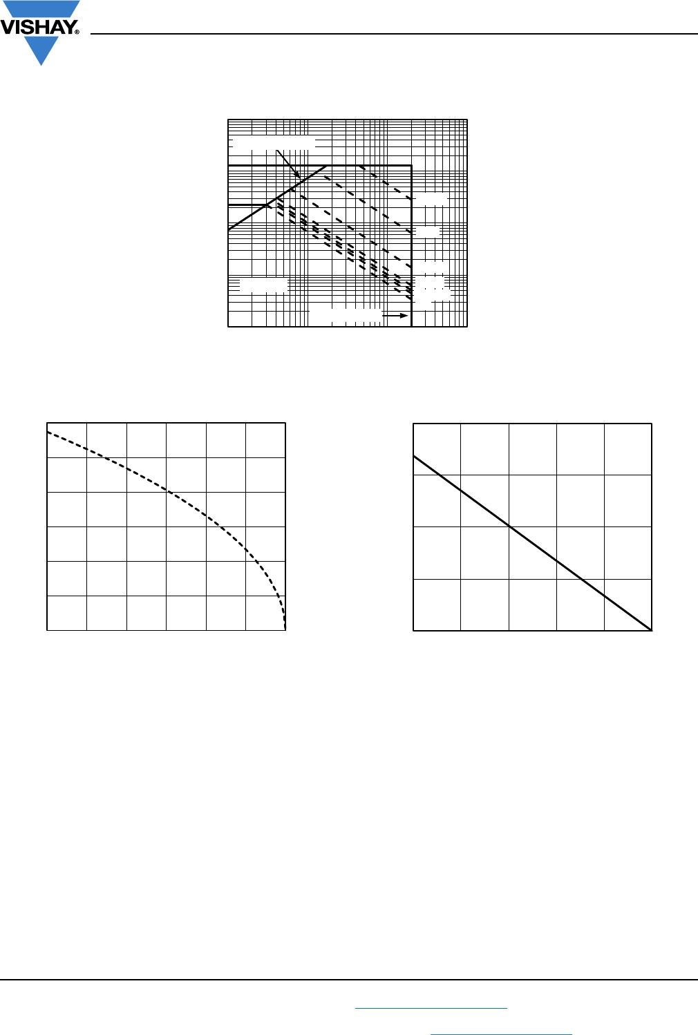
TYPICAL CHARACTERISTICS (25 °C, unless otherwise noted)
Safe Operating Area, Junction-to-Ambient
Current Derating* Power Derating
Note
When mounted on 1" x 1" FR4 with full copper.
* The power dissipation P
D
is based on T
J (max.)
= 150 °C, using junction-to-ambient thermal resistance, and is more useful in
settling the upper dissipation limit for cases where additional heatsinking is used. It is used to determine the current rating, when
this rating falls below the package limit.
0.01
0.1
1
10
100
0.1 1 10 100
I
D
- Drain Current (A)
V
DS
-Drain-to-Source Voltage (V)
* V
GS
> minimum V
GS
at which R
DS(on)
is specied
10 s, 1s
10 ms
100 µs
Limited by R
DS(on)
*
1 ms
T
A
= 25 °C
BVDSS Limited
10 ms
DC
0.0
0.5
1.0
1.5
2.0
2.5
3.0
0 25 50 75 100 125 150
I
D
- Drain Current (A)
T
A
- Ambient Temperature (°C)
0
0.2
0.4
0.6
0.8
25 50 75 100 125 150
Power (W)
T
A
- Ambient Temperature (°C)