NB3N3010BDR2G

NB3N3010B
http://onsemi.com
4
Table 5. AC CHARACTERISTICS V
DD
= 3.3 V $5%, GND = 0 V, T
A
= 0°C to +85°C (Note 4)
Symbol
Characteristic Min Typ Max Unit
f
out
Output Clock Frequency: CLKA & CLKB
f
OUT
= 8 kHz x 1536 S0 = 1
f
OUT
= 4 kHz x 3072 S0 = 0
12.25728
12.25728
12.288
12.288
12.31872
12.31872
MHz
f
REF
Reference Input Frequency S0 = 1
S0 = 0
7.98
3.99
8
4
8.02
4.01
kHz
t
jit(per)ref
Reference Input Period Jitter (pkpk) 250 ns
t
REFH
Reference Input Pulse Width (high) S0 = 1
S0 = 0
33
33
68000
136000
ns
t
CLKH
CLKA, CLKB output width, high 13 ns
t
CLKL
CLKA, CLKB output width, low 13 ns
t
r
CLKA, CLKB rise time 10% 90% 4 ns
t
f
CLKA, CLKB fall time 90% 10% 4 ns
t
jit(per)
CLKA, CLKB period jitter (over 10k cycles) peaktopeak
RMS
250
20
ps
t
jit(cc)
CLK_A, CLKB cycletocycle jitter (1k cycles) peaktopeak
RMS
300
35
ps
t
sk(LH)
CLKA to CLKB output skew (lowtohigh transitions) 700 ps
t
sk(HL)
CLKA to CLKB output skew (hightolow transitions) 700 ps
Power Valid to ENABLEn 10 ms
ENABLEn to CLKA/CLKB 50 100 ms
NOTE: Device will meet the specifications after thermal equilibrium has been established when mounted in a test socket or printed circuit
board with maintained transverse airflow greater than 500 lfpm. Electrical parameters are guaranteed only over the declared
operating temperature range. Functional operation of the device exceeding these conditions is not implied. Device specification limit
values are applied individually under normal operating conditions and not valid simultaneously.
4. Outputs loaded with 15 pF max to ground. C
FILT
capacitor must be installed; see Figure 4.
5. Maximum time required after power is applied to the MCLK FLL until it is ready to accept ENABLEn active.
NB3N3010B
http://onsemi.com
5
APPLICATION INFORMATION
Figure 1 shows the simplified block diagram of the
NB3N3010B device.
The primary function of the NB3N3010B is to accept a
selectable 4 kHz or 8 kHz input reference clock, REF, and
then multiply it to 12.288 MHz output frequency.
Frequency Select SO
Either of two expected input REF frequencies, 4 kHz or
8 kHz, will be multiplied by the FLL to achieve 12.288 MHz
at the lowskew CLKA and CLKB outputs by selecting the
S0 pin; see Table 6.
The pulse high time (T
HI
) of the input reference signal may
vary widely depending on the application. See AC
specifications for details.
Output Enable ENABLEn
A Low active output enable input pin, ENABLEn, is
provided. When the ENABLEn input is High inactive, both
clock outputs are driven to a logic Low.
The NB3N3010B implements a delay, specified as
ENABLEn to Output Delay in the AC Specifications, from
the assertion of ENABLEn to the first rising edges on the
clock outputs. This delay insures that CLKA and CLKB
output pulses are within specification before the output
drivers are enabled. When ENABLEn transitions from Low
to High (deasserts), the current cycle of the clock outputs
completes normally then the outputs will be held Low. The
ENABLEn signal is asynchronous to either the REF input or
CLK_x outputs.
Table 6. INPUT FREQUENCY SELECT AND OUTPUT ENABLE FUNCTIONS
ENABLEn* S0* f
REF
FLL Multiplier CLKA & CLKB Frequency
0 L 4 kHz 3072 12.288 MHz
0 H 8 kHz 1536 12.288 MHz
1 x x x Disabled Low
*Defaults High when left open.
Typical Power On Sequence
1. Power On
2. Reference Clock present; must be switching before ENABLEn goes High.
3. Output Enable, ENABLEn, HightoLow
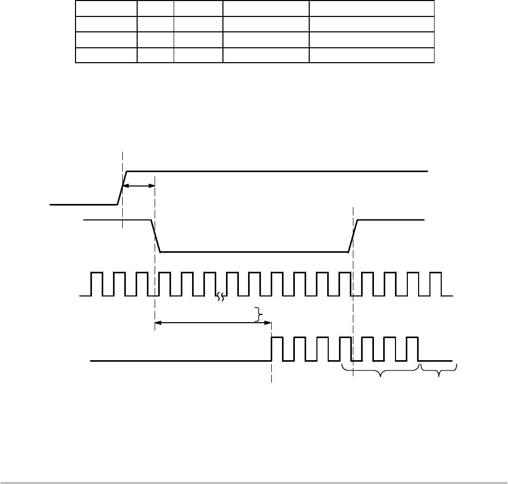
Figure 3. ENABLEn Timing Diagram
V
DD
Valid to ENABLEn
~50 ms, typ
ENABLEn to Output
400 Clock Cycles @ 8 kHz
200 Clock Cycles @ 4 kHz
V
DD
Valid
V
DD
ENABLEn
REF
CLKA/B
Completed Clock
Outputs
Then Low
4 kHz or
8 kHz
12.288 MHz
Outputs Enabled
NB3N3010B
http://onsemi.com
6
CFILT for 1.8 V Regulator
CFILT
1.8 V
Regulator
220 270 nF
Figure 4. CFILT Capacitor
A low noise 1.8 V LDO/Regulator is integrated to provide
a clean supply for the CLKA/CLKB output buffers. The
LDO requires a decoupling capacitor in the range of 220 nF
to 270 nF for compensation and high frequency PSR, and
should be located near the device. The purpose of this design
technique is to isolate the high switching noise of the digital
outputs from the relatively sensitive internal analog
phaselocked loop.
Figure 5. REF Input Timing Diagram
REF
t
REF
T
jitterREF
t
REFH
Figure 6. Clock Output Timing Diagram
T
per
T
jitterPER
T
cyc
t
MCLKL
t
MCLKH
T
jittercyc
T
f
T
f
20%
80%
CLK A, CLK B
VDD
0.1 mF
GND
CLKA
CLKB
15 pF
15 pF
Figure 7. Test Circuit
Bypass Capacitor Close to Pin
HiZ Probe
HiZ Probe

NB3N3010BDR2G

Mfr. #:
Manufacturer:
ON Semiconductor
Description:
Clock Generators & Support Products AUDIO OVERSAMPLING CLOCK
Lifecycle:
New from this manufacturer.
Delivery:
DHL FedEx Ups TNT EMS
Payment:
T/T Paypal Visa MoneyGram Western Union

Products related to this Datasheet