MAX900–MAX903
High-Speed, Low-Power Voltage Comparators
_______________________________________________________________________________________ 9
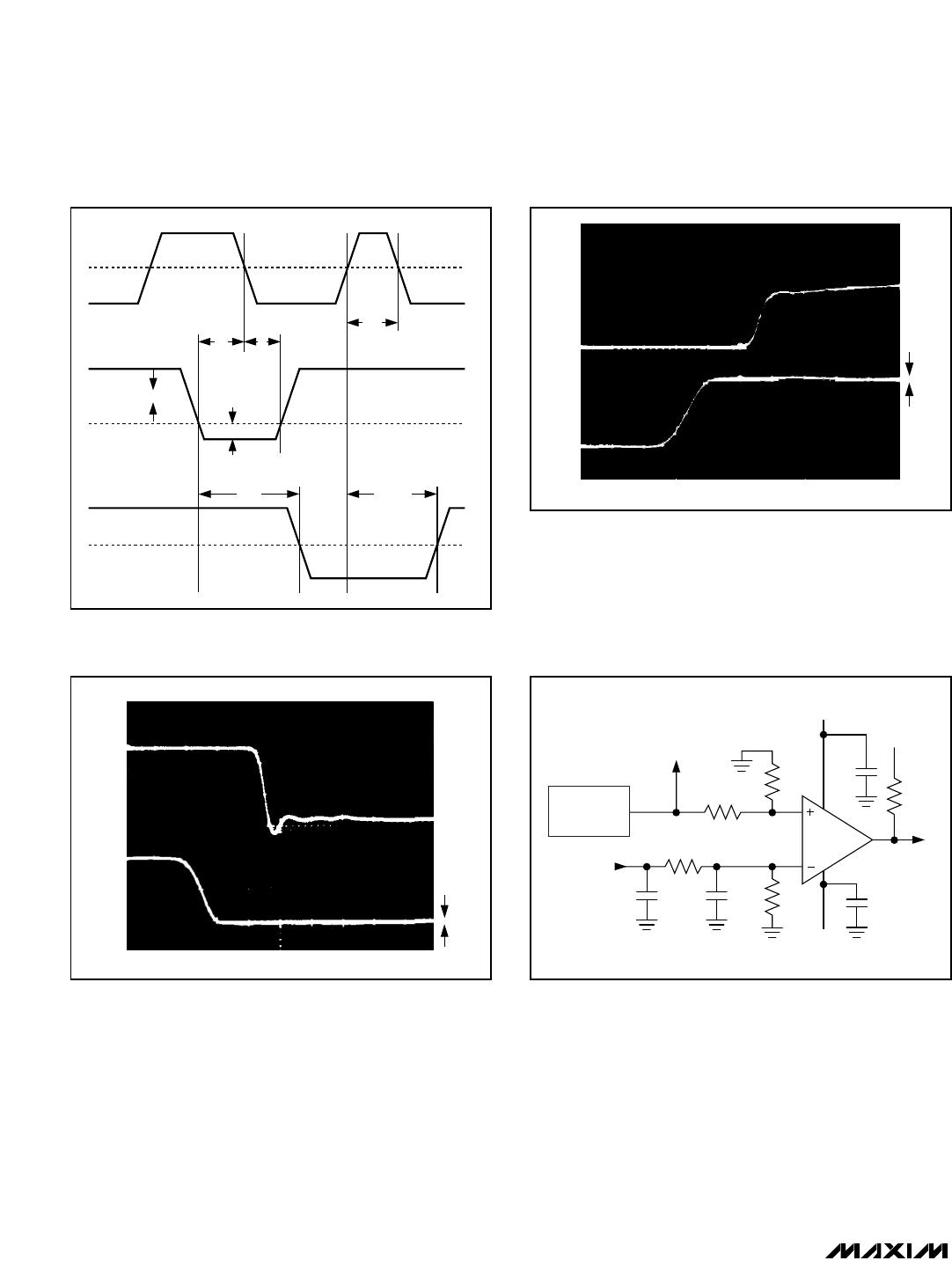
Definitions of Terms
V
OS
Input Offset Voltage: Voltage applied
between the two input terminals to obtain
TTL-logic threshold (+1.4V) at the
output.
t
pd+ (D)
Latch Disable-to-Output High Delay:
The propagation delay measured from
the latch-signal crossing the TTL
threshold in a low-to-high transition to
the point of the output crossing TTL
threshold in a low-to-high transition.
V
IN
Input Voltage Pulse Amplitude: Usually
set to 100mV for comparator
specifications.
t
pd- (D)
Latch Disable-to-Output Low Delay:
The propagation delay measured from
the latch-signal crossing the TTL
threshold in a low-to-high transition to
the point of the output crossing TTL
threshold in a high-to-low transition.
V
OD
Input Voltage Overdrive: Usually set to
5mV and in opposite polarity to V
IN
for
comparator specifications.
t
s
Minimum Setup Time: The minimum
time before the negative transition of the
latch signal that an input signal change
must be present in order to be acquired
and held at the outputs.
t
pd+
Input-to-Output High Delay: The
propagation delay measured from the
time the input signal crosses the input
offset voltage to the TTL-logic threshold
of an output low-to-high transition
t
h
Minimum Hold Time: The minimum time
after the negative transition of the latch
signal that an input signal must remain
unchanged in order to be acquired and
held at the output.
t
pd-
Input-to-Output Low Delay: The
propagation delay measured from the
time the input signal crosses the input
offset voltage to the TTL-logic threshold
of an output high-to-low transition.
t
pw
(D) Minimum Latch-Disable Pulse Width:
The minimum time that the latch signal
must remain high in order to acquire and
hold an input-signal change.
MAX900–MAX903
High-Speed, Low-Power Voltage Comparators
10 ______________________________________________________________________________________
LATCH
ENABLE
INPUT
LATCH LATCH LATCH
COMPARE COMPARE
DIFFERENTAL
INPUT VOLTAGE
COMPARATOR
OUTPUT
V
IN
1.4V
1.4V
V
OS
t
pd+
(D)
tpw(D)
t
pd-
V
DD
t
s
t
h
Figure 2. MAX900/MAX902/MAX903 Timing Diagram
OUTPUT
INPUT
5ns/div
+5V
0
V
OS
+5mV
100mV
Figure 4. t
pd-
Response Time to 5mV Overdrive
PRECISION
STEP GENERATOR
OUTPUT TO 10X
SCOPE PROBE
(10M, 14pF)
INPUT TO 10X
SCOPE PROBE
(10M, 14pF)
100nF
100nF
R
L
2.43k
V
DD
+5V
V
CC
+5V
V
EE
-5V
D.U.T.
10
10
100nF
100nF
V
DC
OFFSET
ADJUST
10k
1k
Figure 5. Response-Time Setup
OUTPUT
INPUT
5ns/div
+5V
0
V
OS
+5mV
100mV
Figure 3. t
pd+
Response Time to 5mV Overdrive
MAX900–MAX903
High-Speed, Low-Power Voltage Comparators
______________________________________________________________________________________ 11
OUTPUT
1V/div
INPUT
10mV/div
5ns/div
Figure 6. Response to 50MHz Sine Wave
MX7228
IN1
UNDER
LIMIT
IN2
IN3
IN4
IN5
IN6
IN8
IN7
OVER
LIMIT
UNDER
LIMIT
UNDER
LIMIT
UNDER
LIMIT
UNDER
LIMIT
OVER
LIMIT
OVER
LIMIT
VDAC8
VDAC1
OCTAL
8-BIT
DAC
8 x 8
DATA
LATCH
CONTROL
LOGIC
A0
A1
A2
MSB
D7
8-BIT
DATA
INPUT
LSB
D1
VREF
+1.25V
V
OUT8
MAX901
V
OUT1
MAX901
Figure 8. Alarm Circuit Level Monitors Eight Separate Inputs
OUTPUT
1V/div
INPUT
10mV/div
5ns/div
Figure 7. Response to 100MHz Sine Wave Photo
Typical Application
Programmed, Variable-Alarm Limits
By combining two quad analog comparators with an
octal 8-bit D/A converter (the MX7228), several alarm
and limit-defect functions can be performed simultane-
ously without external adjustments
The MX7228’s internal latches allow the system
processor to set the limit points for each comparator
independently and update them at any time. Set the
upper and lower thresholds for a single transducer by
pairing the D/A converter and comparator sections.

MAX902ESD+

Mfr. #:
Manufacturer:
Maxim Integrated
Description:
Analog Comparators High-Speed Voltage Comparator
Lifecycle:
New from this manufacturer.
Delivery:
DHL FedEx Ups TNT EMS
Payment:
T/T Paypal Visa MoneyGram Western Union