MAX900–MAX903
High-Speed, Low-Power Voltage Comparators
Typical Operating Characteristics
(T
A
= +25°C, unless otherwise noted.)
0
-1
-2
1
2
200-40 -20 40 60 80 100 120
INPUT OFFSET VOLTAGE
vs. TEMPERATURE
MAX900-03 toc01
TEMPERATURE (
°
C)
INPUT OFFSET VOLTAGE (mV)
3.0
2.5
2.0
3.5
4.0
200-40 -20 40 60 80 100 120
INPUT BIAS CURRENT
vs. TEMPERATURE
MAX900-03 toc02
TEMPERATURE (
°
C)
INPUT BIAS VOLTAGE (µV)
0.2
0.1
0.4
0.3
0.5
OUTPUT LOW VOLTAGE
(V
OL
) vs. LOAD CURRENT
MAX900-03 toc03
LOAD CURRENT (mA)
OUTPUT LOW VOLTAGE (V)
462810
T
A
= -55
°
C
T
A
= +125
°
C
T
A
= +25
°
C
1.8
1.6
2.4
2.2
2.0
3.0
2.8
2.6
6745 8910
I
CC
SUPPLY CURRENT (PER COMPARATOR)
vs. V
CC
SUPPLY VOLTAGE
MAX900-03 toc04
V
CC
SUPPLY VOLTAGE (V)
I
CC
SUPPLY CURRENT (mA)
T
A
= +125
°
C
T
A
= +25
°
C
T
A
= -55
°
C
V
DD
= +5V
0
-100
1
0
100
3
4
2
460 2 8 101214
IINPUT OVERDRIVE vs.
t
pd+
RESPONSE TIME
MAX900-03 toc05
tpd+ RESPONSE TIME (ns)
INPUT VOLTAGE OUTPUT VOLTAGE
INPUT OVERDRIVE (V
OD
)
25mV
2mV
5mV
0
-100
1
0
100
3
4
2
460 2 8 101214
INPUT OVERDRIVE vs.
t
pd-
RESPONSE TIME
MAX900-03 toc06
tpd- RESPONSE TIME (ns)
INPUT VOLTAGE OUTPUT VOLTAGE
INPUT OVERDRIVE (V
OD
)
25mV
2mV
5mV
5
7
6
9
8
10
11
13
12
14
-40 -20 0 20 40 60 80 100 120
RESPONSE TIME vs.
TEMPERATURE (5mV OVERDRIVE)
MAX900-03 toc07
TEMPERATURE (°C)
RESPONSE TIME (ns)
t
pd+
t
pd-
8
7
10
9
11
12
14
13
10 20 30 40 50 60 70 80
RESPONSE TIME vs. LOAD CAPACITANCE
(5mV OVERDRIVE)
MAX900-03 toc08
LOAD CAPACITANCE (pF)
t
pd-
t
pd+
R
L
= 2.4k
6 ______________________________________________________________________________________
MAX900–MAX903
High-Speed, Low-Power Voltage Comparators
_______________________________________________________________________________________ 7
PIN NAME FUNCTION
1, 10, 11, 20 IN- (A, B, C, D)
Negative Input
(Channels A, B, C, D)
2, 9, 12, 19 IN+ (A, B, C, D)
Positive Input
(Channels A, B, C, D)
3 GND Ground Terminal
4, 7, 14, 17
LATCH (A, B, C,
D)
Latch Input (Channels
A, B, C, D)
5, 6, 15, 16 OUT (A, B, C, D)
Output (Channels A, B,
C, D)
8V
EE
Negative Analog
Supply and Substrate
13 V
DD
Positive Digital Supply
18 V
CC
Positive Analog Supply
PIN NAME FUNCTION
1, 8 IN- (A, B)
Negative Input
(Channels A, B)
2, 9 IN+ (A, B)
Positive Input
(Channels A, B)
3 GND Ground Terminal
4, 11 LATCH (A, B)
Latch Input (Channels
A, B)
5, 12 OUT (A, B) Output (Channels A, B)
6, 13 N.C.
No Connection. Not
internally connected.
7V
EE
Negative Analog
Supply and Substrate
10 V
DD
Positive Digital Supply
14 V
CC
Positive Analog Supply
PIN NAME FUNCTION
1V
CC
Positive Analog Supply
2 IN+ Positive Input
3 IN- Negative Input
4V
EE
Negative Analog
Supply and Substrate
5 LATCH Latch Input
6 GND Ground Terminal
7 OUT Output
8V
DD
Positive Digital Supply
PIN NAME FUNCTION
1, 8, 9, 16 IN- (A, B, C, D)
Negative Input
(Channels A, B, C, D)
2, 7, 10, 15 IN+ (A, B, C, D)
Positive Input
(Channels A, B, C, D)
3 GND Ground Terminal
4, 5, 12, 13 OUT (A, B, C, D)
Output (Channels A,
B, C, D)
6V
EE
Negative Analog
Supply and Substrate
11 V
DD
Positive Digital Supply
14 V
CC
Positive Analog
Supply
Pin Descriptions
MAX900
MAX901
MAX902
MAX903
MAX900–MAX903
High-Speed, Low-Power Voltage Comparators
8 _______________________________________________________________________________________
Applications Information
Circuit Layout
Because of the large gain-bandwidth transfer function of
the MAX900–MAX903, special precautions must be
taken to realize their full high-speed capability. A printed
circuit board with a good, low-inductance ground plane
is mandatory. All decoupling capacitors (the small
100nF ceramic type is a good choice) should be mount-
ed as close as possible to the power-supply pins.
Separate decoupling capacitors for analog V
CC
and for
digital V
DD
are also recommended. Close attention
should be paid to the bandwidth of the decoupling and
terminating components. Short lead lengths on the
inputs and outputs are essential to avoid unwanted par-
asitic feedback around the comparators. Solder the
device directly to the printed circuit board instead of
using a socket.
Input Slew-Rate Requirements
As with all high-speed comparators, the high gain-band-
width product of the MAX900–MAX903 can create oscil-
lation problems when the input traverses the linear
region. For clean output switching without oscillation or
steps in the output waveform, the input must meet mini-
mum slew-rate requirements. Oscillation is largely a
function of board layout and of coupled source imped-
ance and stray input capacitance. Both poor layout and
large-source impedance will cause the part to oscillate
and increase the minimum slew-rate requirement. In
some applications, it may be helpful to apply some posi-
tive feedback between the output and + input. This
pushes the output through the transition region cleanly,
but applies a hysteresis in threshold seen at the input
terminals.
TTL Output and Latch Inputs
The comparator TTL-output stages are optimized for dri-
ving low-power Schottky TTL with a fan-out of four.
When the latch is connected to a logic high level, the
comparator is transparent and immediately responds to
changes at the input terminals. When the latch is con-
nected to a TTL low level, the comparator output latches
in the same state as at the instant that the latch command
is applied, and will not respond to subsequent changes
at the input. No latch is provided on the MAX901.
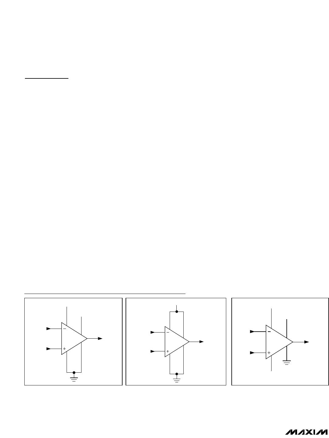
Power Supplies
The MAX900–MAX903 can be powered from separate
analog and digital supplies or from a single +5V supply.
The analog supply can range from +5V to +10V with
V
EE
grounded for single-supply operation (Figures 1A
and 1B) or from a split ±5V supply (Figure 1C). The V
DD
digital supply always requires +5V.
In high-speed, mixed-signal applications where a com-
mon ground is shared, a noisy digital environment can
adversely affect the analog input signal. When set up
with separate supplies (Figure 1C), the
MAX900–MAX903 isolate analog and digital signals by
providing a separate AGND (V
EE
) and DGND.
+10V
+5V
V
CC
V
EE
V
DD
OUT
GND
+5V
V
CC
V
EE
V
DD
OUT
GND
+5V
-5V
+5V
V
CC
V
EE
V
DD
OUT
GND
Figure 1A. Separate Analog Supply,
Common Ground
Figure 1B. Single +5V Supply, Common
Ground
Figure 1C. Split ±5V Supply, Separate
Ground
Typical Power-Supply Alternatives

MAX902ESD+

Mfr. #:
Manufacturer:
Maxim Integrated
Description:
Analog Comparators High-Speed Voltage Comparator
Lifecycle:
New from this manufacturer.
Delivery:
DHL FedEx Ups TNT EMS
Payment:
T/T Paypal Visa MoneyGram Western Union