LTC1164-5
1
11645fc
Low Power 8th Order
Pin Selectable Butterworth
or Bessel Lowpass Filter
Butterworth 20kHz Anti-Aliasing Filter
Pin Selectable Butterworth or Bessel Response
4mA Supply Current with ±5V Supplies
f
CUTOFF
up to 20kHz
100µV
RMS
Wideband Noise
THD < 0.02% (50:1, V
S
= ±7.5V, V
IN
= 2V
RMS
)
Operates with a Single 5V Supply (1V
RMS
Input
Range)
60µV
RMS
Clock Feedthrough (Single 5V Supply)
Operates up to ±8V Supplies
TTL/CMOS-Compatible Clock Input
No External Components
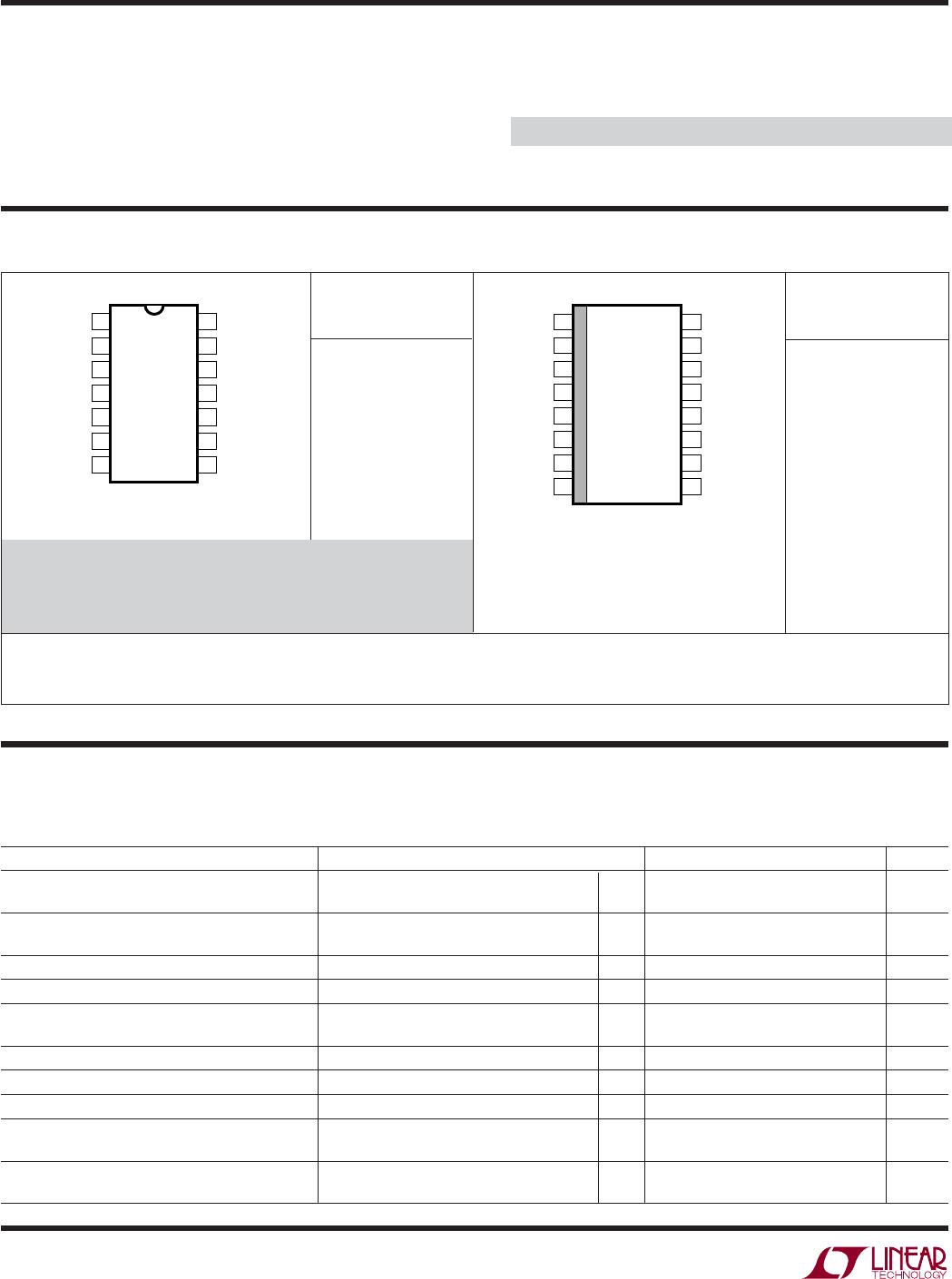
Available in 14-Pin DIP and 16-Pin SO Wide
Packages
The LTC
®
1164-5 is a monolithic 8th order filter; it approxi-
mates either a Butterworth or a Bessel lowpass response.
The LTC1164-5 features clock-tunable cutoff frequency
and low power consumption (4.5mA with ±5V supplies
and 2.5mA with single 5V supply).
Low power operation is achieved without compromising
noise or distortion performance. With ±5V supplies and
10kHz cutoff frequency, the operating signal-to-noise
ratio is 86dB and the THD throughout the passband is
0.015%. Under the same conditions, a 77dB signal-to-
noise ratio and distortion is obtained with a single 5V
supply while the clock feedthrough is kept below the noise
level. The maximum signal-to-noise ratio is 92dB.
The LTC1164-5 approximates an 8th order Butterworth
response with a clock-to-cutoff frequency ratio of 100:1
(Pin 10 to V
) or 50:1 double-sampled (Pin 10 to V
+
and
Pin 1 shorted to Pin 13). Double-sampling allows the input
signal frequency to reach the clock frequency before any
aliasing occurrence. An 8th order Bessel response can
also be approximated with a clock-to-cutoff frequency
ratio of 140:1 (Pin 10 to ground). With ±7.5V supply, ±5V
supply and single 5V supply, the maximum clock fre-
quency of the LTC1164-5 is 1.5MHz, 1MHz and 1MHz
respectively. The LTC1164-5 is pin-compatible with the
LTC1064-2 and LTC-1064-3.
Frequency Response
Anti-Aliasing Filters
Battery-Operated Instruments
Telecommunications Filters
Smoothing Filters
FEATURES
APPLICATIO S
U
DESCRIPTIO
U
TYPICAL APPLICATIO
U
, LTC and LT are registered trademarks of Linear Technology Corporation.
All other trademarks are the property of their respective owners.
FREQUENCY (kHz)
1
GAIN (dB)
0
–10
–20
–30
–40
–50
–60
–70
–80
10 100
1164-5 TA02
1
2
3
4
5
6
7
14
13
12
11
10
9
8
LTC1164-5
V
IN
8V
NC
–8V
CLK = 1MHz
TO V
+
V
OUT
WIDEBAND NOISE = 110µV
RMS
THD IN PASSBAND < 0.02% AT V
IN
= 2V
RMS
NOTE: THE CONNECTION FROM PIN 7 TO PIN 14
SHOULD BE MADE UNDER THE PACKAGE.
FOR 50:1 OPERATION CONNECT PIN 1 TO PIN 13
AS SHOWN. FOR 100:1 OR 150:1 OPERATION PINS 1
AND 13 SHOULD FLOAT. THE POWER SUPPLIES
SHOULD BE BYPASSED BY A 0.1µF CAPACITOR AS
CLOSE TO THE PACKAGE AS POSSIBLE.
1164-5 TA01
LTC1164-5
2
11645fc
ELECTRICAL CHARACTERISTICS
The denotes the specifications which apply over the full operating
temperature range, otherwise specifications are at T
A
= Operating Temperature Range. V
S
= ±7.5V, R
L
= 10k, f
CLK
= 400kHz,
unless otherwise specified.
1
2
3
4
5
6
7
8
TOP VIEW
SW PACKAGE
16-LEAD PLASTIC SO WIDE
16
15
14
13
12
11
10
9
50:1 MODE
V
IN
GND
V
+
GND
NC
LP6
CONNECT 1
CONNECT 2
50:1 MODE
V
NC
CLK
BUTT/BESS
NC
V
OUT
1
2
3
4
5
6
7
TOP VIEW
N PACKAGE
14-LEAD PDIP
14
13
12
11
10
9
8
50:1 MODE
V
IN
GND
V
+
GND
LP6
CONNECT 1
CONNECT 2
50:1 MODE
V
CLK
BUTT/BESS
V
OUT
NC
Total Supply Voltage (V
+
to V
) ............................. 16V
Input Voltage (Note 2) ......... (V
+
+ 0.3V) to (V
0.3V)
Output Short-Circuit Duration ......................... Indefinite
Power Dissipation............................................. 400mW
Burn-In Voltage ...................................................... 16V
Operating Temperature Range
LTC1164-5C ...................................... 40°C to 85°C
LTC1164-5M (OBSOLETE) ............... 55°C to 125°C
Storage Temperature Range ................ 65°C to 150°C
Lead Temperature (Soldering, 10 sec)................. 300°C
ABSOLUTE AXI U RATI GS
W
WW
U
(Note 1)
PARAMETER CONDITIONS MIN TYP MAX UNITS
Passband Gain 0.1Hz at 0.25f
CUTOFF
(Note 3) f
IN
= 1kHz, (f
CLK
/f
C
) = 100:1 0.5 0.10 0.25 dB
f
IN
= 1kHz, (f
CLK
/f
C
) = 50:1 0.5 0.10 0.25 dB
Gain at 0.50f
CUTOFF
(Note 3) f
IN
= 2kHz, (f
CLK
/f
C
) = 100:1 0.45 0.20 0.17 dB
f
IN
= 4kHz, (f
CLK
/f
C
) = 50:1 0.35 0.10 0.40 dB
Gain at 0.90f
CUTOFF
(Note 3) f
IN
= 3.6kHz, (f
CLK
/f
C
) = 100:1 2.50 –1.90 –1.0 dB
Gain at 0.95f
CUTOFF
(Note 3) f
IN
= 3.8kHz, (f
CLK
/f
C
) = 100:1 2.60 dB
Gain at f
CUTOFF
(Note 3) f
IN
= 4kHz, (f
CLK
/f
C
) = 100:1 4.10 3.40 2.75 dB
f
IN
= 8kHz, (f
CLK
/f
C
) = 50:1 4.20 3.80 2.75 dB
Gain at 1.44f
CUTOFF
(Note 3) f
IN
= 5.76kHz, (f
CLK
/f
C
) = 100:1 20.5 –19.0 –17.0 dB
Gain at 2.0f
CUTOFF
(Note 3) f
IN
= 8kHz, (f
CLK
/f
C
) = 100:1 45.0 43.0 41.0 dB
Gain with f
CLK
= 20kHz (Note 3) f
IN
= 200Hz, (f
CLK
/f
C
) = 100:1 4.50 3.40 2.75 dB
Gain with V
S
= 2.375V (Note 3) f
IN
= 400kHz, f
IN
= 2kHz, (f
CLK
/f
C
) = 100:1 0.50 0.10 0.35 dB
f
IN
= 400kHz, f
IN
= 4kHz, (f
CLK
/f
C
) = 100:1 4.20 3.40 2.00 dB
Input Frequency Range (f
CLK
/f
C
) = 100:1 0 – <f
CLK
/2 kHz
(f
CLK
/f
C
) = 50:1 0 – <f
CLK
kHz
ORDER PART
NUMBER
ORDER PART
NUMBER
T
JMAX
= 110°C,
θ
JA
= 85°C/W
LTC1164-5CN LTC1164-5CSW
PACKAGE/ORDER I FOR ATIO
UUW
T
JMAX
= 110°C,
θ
JA
= 65°C/W
Consult LTC Marketing for parts specified with wider operating temperature ranges.
LTC1164-5CJ
LTC1164-5MJ
J PACKAGE 14-LEAD CERDIP
T
JMAX
= 110°C,
θ
JA
= 65°C/W
OBSOLETE PACKAGE
Consider the N Package as an Alternate Source
Order Options Tape and Reel: Add #TR
Lead Free: Add #PBF Lead Free Tape and Reel: Add #TRPBF
Lead Free Part Marking: http://www.linear.com/leadfree/
LTC1164-5
3
11645fc
FREQUENCY (kHz)
0.2
GAIN (dB)
–5
0
1.0
1164-5 G02
–10
–15
0.4
0.6
0.8
–90
0
180
270
PHASE (DEG)
GAIN
PHASE
V
S
= ±5V
f
CLK
= 50kHz
f
CUTOFF
= 1kHz
(50:1, PIN 10 TO V
+
,
PINS 1-13 SHORTED)
T
A
= 25°C
FREQUENCY (kHz)
0.1
–50
GAIN (dB)
–40
–30
–20
–10
110
1164-5 G01
–60
–70
–80
0
A. f
CLK
= 100kHz
f
CUTOFF
= 1kHz
(100:1, PIN 10 TO V
)
B. f
CLK
= 375kHz
f
CUTOFF
= 2.68kHz
(140:1, PIN 10 GND)
C. f
CLK
= 500kHz
f
CUTOFF
= 10kHz
(50:1, PIN 10 TO V
+
,
PINS 1-13 SHORTED)
ACB
V
S
= ±5V
T
A
= 25°C
50
LTC1164-5C
PARAMETER CONDITIONS MIN TYP MAX UNITS
Maximum f
CLK
V
S
±7.5V 1.5 MHz
V
S
= ±5.0V 1.0 MHz
V
S
= Single 5V (GND = 2V) 1.0 MHz
Clock Feedthrough Input at GND, f = f
CLK
, Square Wave
±5V, (f
CLK
/f
C
) = 100:1 200 µV
RMS
±5V, (f
CLK
/f
C
) = 50:1 100 µV
RMS
Wideband Noise Input at GND, 1Hz f < f
CLK
±5V, (f
CLK
/f
C
) = 100:1 100 ±5% µV
RMS
±5V, (f
CLK
/f
C
) = 50:1 115 ±5% µV
RMS
Input Impedance 70 100 160 k
Output DC Voltage Swing V
S
= ±2.375V ±1.25 ±1.50 V
V
S
= ±5.0V ±3.70 ±4.10 V
V
S
= ±7.5V ±5.40 ±5.90 V
Output DC Offset V
S
= ±5V, (f
CLK
/f
C
) = 100:1 ± 50 ±160 mV
Output DC Offset TempCo V
S
= ±5V, (f
CLK
/f
C
) = 100:1 ±100 µV/°C
Power Supply Current V
S
= ±2.375V, T
A
25°C 2.5 4.0 mA
4.5 mA
V
S
= ±5.0V, T
A
25°C 4.5 7.0 mA
8.0 mA
V
S
= ±7.5V, T
A
25°C 7.0 11.0 mA
12.5 mA
Power Supply Range ±2.375 ±8V
TYPICAL PERFOR A CE CHARACTERISTICS
UW
Note 1: Absolute Maximum Ratings are those values beyond which life of
the device may be impaired.
Note 2: Connecting any pin to voltages greater than V
+
or less than V
may cause latch-up. It is recommended that no sources operating from
external supplies be applied prior to power-up of the LTC1164-5.
Note 3: All gains are measured relative to passband gain. The filter cutoff
frequency is abbreviated as f
CUTOFF
or f
C
.
Gain vs Frequency
Passband Gain and Phase
vs Frequency
ELECTRICAL CHARACTERISTICS
The denotes the specifications which apply over the full operating
temperature range, otherwise specifications are at T
A
= Operating Temperature Range. V
S
= ±7.5V, R
L
= 10k, f
CLK
= 400kHz,
unless otherwise specified.

LTC1164-5CSW#TRPBF

Mfr. #:
Manufacturer:
Analog Devices Inc.
Description:
Active Filter L/P Clk Sweepable Butterworth Filter
Lifecycle:
New from this manufacturer.
Delivery:
DHL FedEx Ups TNT EMS
Payment:
T/T Paypal Visa MoneyGram Western Union

Products related to this Datasheet