LTC1164-5
7
11645fc
POWER SUPPLY (V
+
OR V
)
0
CURRENT (mA)
12
11
10
9
8
7
6
5
4
3
2
1
0
13 68
1164-5 G29
1024579
–55°C
25°C
125°C
FREQUENCY (Hz)
20
–90
PSRR (dB)
–70
–50
–30
–10
100
1164-5 G28
–80
–60
–40
–20
0
10
1k
10k
50k
f
CUTOFF
= 1kHz
V
V
+
FREQUENCY (FREQUENCY/f
CUTOFF
)
0
0
TOTAL PHASE DIFFERENCE (DEG)
2
4
6
8
10
0.2
0.4 0.6 0.8
1164-5 G27
1.0 1.2
MAXIMUM PHASE DIFFERENCE
BETWEEN ANY TWO UNITS
(SAMPLE OF 50 UNITS)
V
S
±5V
T
A
70°C
f
CLK
500KHz
A
B
A. BUTTERWORTH
(f
CLK
/f
CUTOFF
= 100:1 OR 50:1)
B. BESSEL (f
CLK
/f
CUTOFF
= 140:1)
INPUT (V
RMS
)
0.50
THD + NOISE (dB)
–60
–50
–45
1.25
1164-5 G26
–70
–80
–90
0.75 1.00
1.50
–55
–40
–65
–75
–85
f
CLK
= 1MHz
T
A
=25°C
GND = 2V
GND = 2.5V
FREQUENCY (kHz)
2
PHASE (DEG)
0
1.0
2.0
18
1164-5 G25
1.0
2.0
3.0
6
10
16
22
201412
84
2.5
1.5
0.5
0.5
1.5
T
A
= 70°C
f
CLK
= 1MHz
GND = 2.5V
GND = 2V
INPUT VOLTAGE (V
RMS
)
0.1
THD + WIDEBAND NOISE (dB)
1164-5 G24
1
5
–50
–54
–58
–62
–66
–70
–74
–78
–82
–86
–90
f
IN
= 1kHz, 140:1
f
CLK
= 750kHz
V
S
= ±2.5V
V
S
= ±7.5V
V
S
= ±5V
THD + Noise vs Input Voltage
THD + Noise vs RMS Input for
Single 5V, 50:1
Maximum Passband for Single 5V,
50:1, for Two Ground Bias Levels
Power Supply Rejection Ratio
vs FrequencyPhase Matching vs Frequency
Power Supply Current vs Power
Supply Voltage
Transient Response
V
IN
= ±3V, 500Hz Square Wave
Transient Response
V
IN
= ±3V, 500Hz Square Wave
BUTTERWORTH RATIO = 100:1
f
CLK
= 500kHz
f
C
= 5kHz
V
S
= ±7.5V
BESSEL RATIO = 140:1
f
CLK
= 700kHz
f
C
= 5kHz
V
S
= ±7.5V
2V/DIV
1164-5 G30
1164-5 G31
2V/DIV
500µs/DIV
500µs/DIV
TYPICAL PERFOR A CE CHARACTERISTICS
UW
LTC1164-5
8
11645fc
1
2
3
4
5
6
7
14
13
12
11
10
9
8
V
IN
5V V
+
16V
1k
V
OUT
DIGITAL SUPPLY
+
GND
CLOCK SOURCE
1164-5 F02
+
LTC1164-5
0.1µF
1µF
10k
10k
1
2
3
4
5
6
7
14
13
12
11
10
9
8
V
IN
V
+
1k
V
V
OUT
LTC1164-5
DIGITAL SUPPLY
+
GND
CLOCK SOURCE
*
1164-5 F01
* OPTIONAL (SEE TEXT)
0.1µF
0.1µF
Power Supply (Pins 4, 12)
The V
+
(Pin 4) and the V
(Pin 12) should be bypassed with
a 0.1µF capacitor to an adequate analog ground. The
filter’s power supplies should be isolated from other
digital or high voltage analog supplies. A low noise linear
supply is recommended. Using a switching power supply
will lower the signal-to-noise ratio of the filter. The supply
during power-up should have a slew rate less than 1V/µs.
When V
+
is applied before V
, and V
can be more positive
than ground, a signal diode must be used to clamp V
.
Figures 1 and 2 show typical connections for dual and
single supply operation.
Clock Input (Pin 11)
Any TTL or CMOS clock source with a square-wave output
and 50% duty cycle (±10%) is an adequate clock source
for the device. The power supply for the clock source
should not be the filter’s power supply. The analog ground
for the filter should be connected to clock’s ground at a
single point only. Table 1 shows the clock’s low and high
level threshold value for a dual or single supply operation.
A pulse generator can be used as a clock source provided
the high level ON time is greater than 0.5µs. Sine waves are
not recommended for clock input frequencies less than
100kHz, since excessively slow clock rise or fall times
generate internal clock jitter (maximum clock rise or fall
time 1µs). The clock signal should be routed from the
right side of the IC package to avoid coupling into any input
or output analog signal path. A 1k resistor between clock
source and Pin 11 will slow down the rise and fall times of
the clock to further reduce charge coupling, Figures 1
and 2.
Table 1. Clock Source High and Low Threshold Levels
POWER SUPPLY HIGH LEVEL LOW LEVEL
Dual Supply > ±3.4V V
+
/3 0.5V
Dual Supply ±3.4V V
+
/3 V
+ 0.5V
Single Supply V
+
> 6.8V, V
= 0V V
+
• 0.65 0.5V + 1/2V
+
Single Supply V
+
< 6.8V, V
= 0V V
+
/3 0.5V
Analog Ground (Pins 3, 5)
The filter performance depends on the quality of the
analog signal ground. For either dual or single supply
operation, an analog ground plane surrounding the pack-
age is recommended. The analog ground plane should be
connected to any digital ground at a single point. For dual
supply operation, Pins 3 and 5 should be connected to the
analog ground plane. For single supply operation Pins 3
and 5 should be biased at 1/2 supply and they should be
bypassed to the analog ground plane with at least a 1µF
capacitor (Figure 2). For single 5V operation at the highest
f
CLK
of 1MHz, Pins 3 and 5 should be biased at 2V. This
minimizes passband gain and phase variations (see Typi-
cal Performance Characteristics curves: Maximum Pass-
band for Single 5V, 50:1; and THD + Noise vs RMS Input
for Single 5V, 50:1).
PI FU CTIO S
UUU
Figure 1. Dual Supply Operation for f
CLK
/f
CUTOFF
= 100:1
Figure 2. Single Supply Operation for f
CLK
/f
CUTOFF
= 100:1
LTC1164-5
9
11645fc
1k
1164-5 F03
+
LT1056
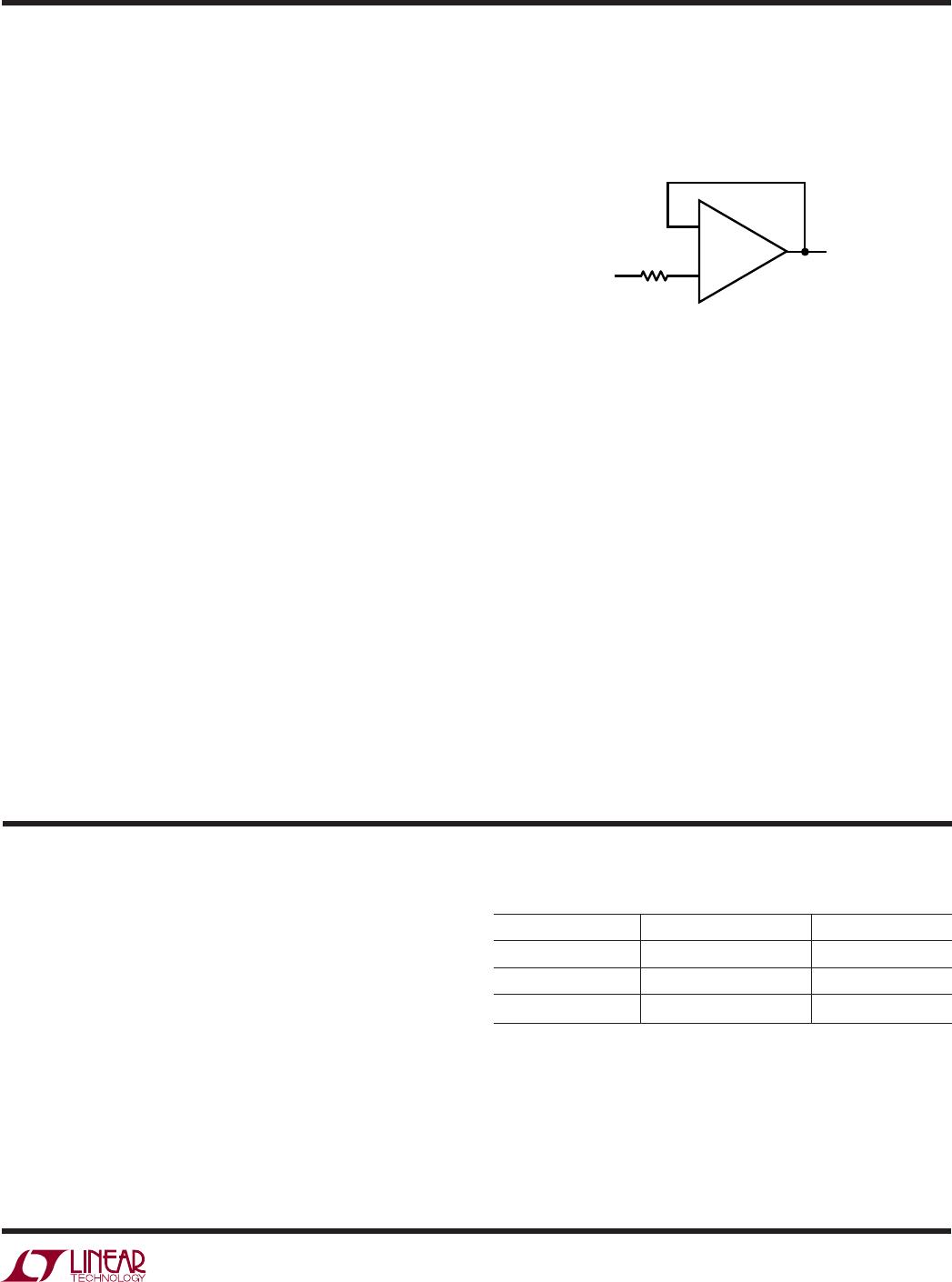
Figure 3. Buffer for Filter Output
PI FU CTIO S
UUU
Butterworth/Bessel (Pin 10)
The DC level at Pin 10 determines the ratio of the clock
frequency to the cutoff frequency of the filter. Pin 10 at V
+
gives a 50:1 ratio and a Butterworth response (pins 1 to 13
are shorted for 50:1 only). Pin 10 at V
gives a 100:1
Butterworth response. Pin 10 at ground gives a Bessel
response and a ratio of 140:1. For single supply operation
the ratio is 50:1 when Pin 10 is at V
+
(Pins 1 to 13 shorted),
100:1 when Pin 10 is at ground, and 140:1 when at 1/2
supply. When Pin 10 is not tied to ground, it should be
bypassed to analog ground with a 0.1µF capacitor. If the
DC level at Pin 10 is switched mechanically or electrically
at slew rates greater than 1V/µs while the device is
operating, a 10k resistor should be connected between
Pin 10 and the DC source.
Filter Input (Pin 2)
The input pin is connected internally through a 100k
resistor tied to the inverting input of an op amp.
Filter Output (Pins 9, 6)
Pin 9 is the specified output of the filter; it can typically
source or sink 1mA. Driving coaxial cables or resistive
loads less than 20k will degrade the total harmonic distor-
tion of the filter. When evaluating the device’s distortion an
output buffer is required. A noninverting buffer, Figure 3,
can be used provided that its input common mode range
is well within the filter’s output swing. Pin 6 is an interme-
diate filter output providing an unspecified 6th order
lowpass filter. Pin 6 should not be loaded.
External Connection (Pins 7, 14 and 1, 13)
Pins 7 and 14 should be connected together. In a printed
circuit board the connection should be done under the IC
package through a short trace surrounded by the analog
ground plane. When the clock to cutoff frequency ratio is
set at 50:1, Pin 1 should be shorted to Pin 13; if not, the
passband will exhibit 1dB of gain peaking and it will deviate
from a Butterworth response. Pin 1 is the inverting input
of an internal op amp and it should preferably be 0.2 inches
away from any other circuit trace.
NC (Pin 8)
Pin 8 is not connected to any internal circuit point on the
device and should be preferably tied to analog ground.
Table 2. Output Clock Feedthrough
V
S
50:1 100:1
±2.5V 60µV
RMS
60µV
RMS
±5V 100µV
RMS
200µV
RMS
±7.5V 150µV
RMS
500µV
RMS
Note: The clock feedthrough at ±2.5V supplies is imbedded in the
wideband noise of the filter. The clock waveform is a square wave.
APPLICATIO S I FOR ATIO
WUU
U
Clock Feedthrough
Clock feedthrough is defined as, the RMS value of the
clock frequency and its harmonics that are present at the
filter’s output pin (Pin 9). The clock feedthrough is tested
with the input pin (Pin 2) grounded and, it depends on PC
board layout and on the value of the power supplies. With
proper layout techniques the values of the clock feedthrough
are shown in Table 2.

LTC1164-5CSW#TRPBF

Mfr. #:
Manufacturer:
Analog Devices Inc.
Description:
Active Filter L/P Clk Sweepable Butterworth Filter
Lifecycle:
New from this manufacturer.
Delivery:
DHL FedEx Ups TNT EMS
Payment:
T/T Paypal Visa MoneyGram Western Union

Products related to this Datasheet