IRF9Z30PBF

IRF9Z30, SiHF9Z30
www.vishay.com
Vishay Siliconix
S12-3048-Rev. A, 24-Dec-12
4
Document Number: 91459
For technical questions, contact: hvm@vishay.com
THIS DOCUMENT IS SUBJECT TO CHANGE WITHOUT NOTICE. THE PRODUCTS DESCRIBED HEREIN AND THIS DOCUMENT
ARE SUBJECT TO SPECIFIC DISCLAIMERS, SET FORTH AT www.vishay.com/doc?91000
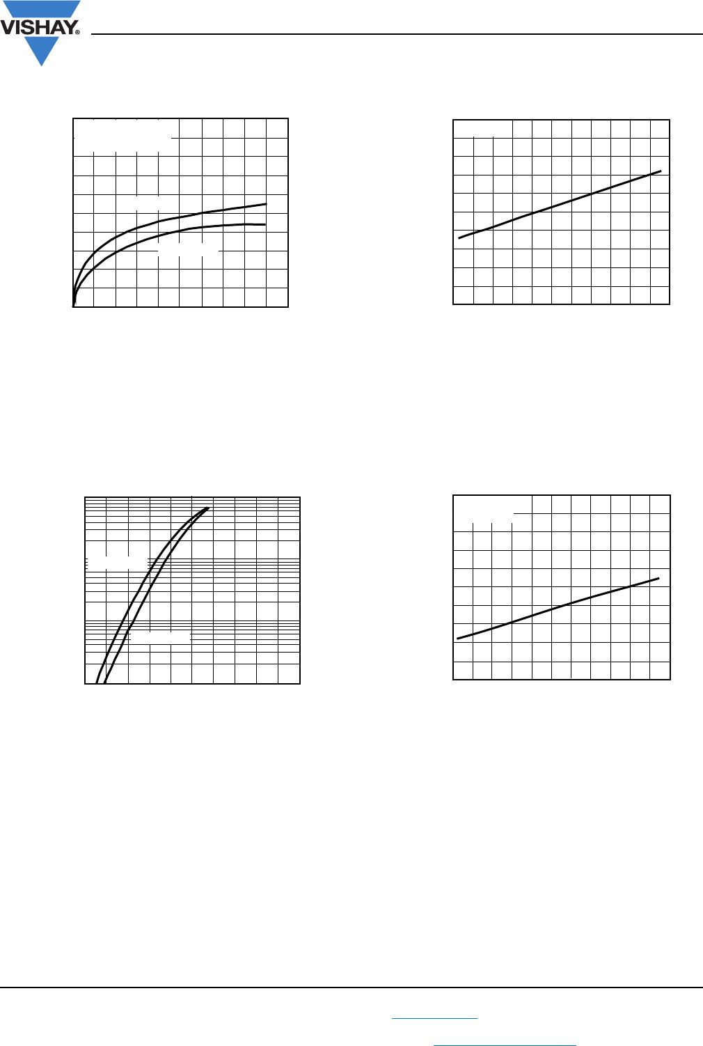
Fig. 5 - Typical Transconductance vs. Drain Current
Fig. 6 - Typical Source-Drain Diode Forward Voltage
Fig. 7 - Breakdown Voltage vs. Temperature
Fig. 8 - Normalized On-Resistance vs. Temperature
- V
SD
, Source-to-Drain Voltage (V)
- I
SD
, Reverse Drain Current (A)
T
J
= 25 °C
T
J
= 150 °C
0
2
4
68
10
10
2
5
2
10
5
2
1
5
2
0.1
T
J
, Junction Temperature (°C)
V
DS
, Drain-to-Source Breakdown
1.25
Voltage (Normalized)
1.15
0.75
0.85
0.95
1.05
- 60 - 40 - 20 0 20 40 60 80 100
120
140 160
I
D
= 1 mA
T
J
, Junction Temperature (°C)
R
DS(on)
, Drain-to-Source On Resistance
3.0
(Normalized)
2.4
0.0
0.6
1.2
1.8
- 60 - 40 - 20 0 20 40 60 80 100 120 140 160
I
D
= - 18 A
V
GS
= - 10 V
IRF9Z30, SiHF9Z30
www.vishay.com
Vishay Siliconix
S12-3048-Rev. A, 24-Dec-12
5
Document Number: 91459
For technical questions, contact: hvm@vishay.com
THIS DOCUMENT IS SUBJECT TO CHANGE WITHOUT NOTICE. THE PRODUCTS DESCRIBED HEREIN AND THIS DOCUMENT
ARE SUBJECT TO SPECIFIC DISCLAIMERS, SET FORTH AT www.vishay.com/doc?91000
Fig. 9 - Typical Capacitance vs. Drain-to-Source Voltage
Fig. 10 - Typical Gate Charge vs. Gate-to-Source Voltage
Fig. 11 - Typical On-Resistance vs. Drain Current
Fig. 12 - Maximum Drain Current vs. Case Temperature
Capacitance (pF)
- V
DS
,
Drain-to-Source Voltage (V)
C
iss
C
oss
C
rss
1
2
5
2
10
2
10
5
0
800
1200
1600
2000
400
V
GS
= 0 V, f = 1 MHz
C
iss
= C
gs
+ C
gd
, C
ds
Shorted
C
rss
= C
gd
C
oss
= C
ds
+ C
gd
Q
g
, Total Gate Charge (nC)
- V
GS
, Gate-to-Source Voltage (V)
20
16
12
8
0
4
I
D
= - 18 A
V
DS
= - 40 V
For test circuit
see gure 17
10
020
30 40 50
80 μ
s Pulse Test
V
GS
= - 10 V
V
GS
= - 20 V
0
12 24 36 48
60
0.4
0.8
1.2
1.6
2.0
- I
D
, Drain Current (A)
R
DS(on)
, Drain to Source on Resistance
0.0
- I
D
, Drain Current (A)
T
C
, Case Temperature (°C)
25 1501251007550
SiHF9Z32
SiHF9Z30
0
4
8
12
16
20
IRF9Z30, SiHF9Z30
www.vishay.com
Vishay Siliconix
S12-3048-Rev. A, 24-Dec-12
6
Document Number: 91459
For technical questions, contact: hvm@vishay.com
THIS DOCUMENT IS SUBJECT TO CHANGE WITHOUT NOTICE. THE PRODUCTS DESCRIBED HEREIN AND THIS DOCUMENT
ARE SUBJECT TO SPECIFIC DISCLAIMERS, SET FORTH AT www.vishay.com/doc?91000
Fig. 13a - Unclamped Inductive Test Circuit
Fig. 13b - Unclamped Inductive Load Test Waveforms
Fig. 14 - Maximum Effective Transient Thermal Impedance, Junction-to-Case vs. Pulse Duration
Fig. 15 - Switching Time Test Circuit Fig. 16 - Gate Charge Test Circuit
Vishay Siliconix maintains worldwide manufacturing capability. Products may be manufactured at one of several qualified locations. Reliability data for Silicon
Technology and Package Reliability represent a composite of all qualified locations. For related documents such as package/tape drawings, part marking, and
reliability data, see www.vishay.com/ppg?91459
.
Vary t
p
to obtain
required peak I
L
V
DD
= 0 5 8 V
DS
E
C
= 0 75 BV
DS
-
+
V
DD
L
E
C
DUT
I
L
V
GS
= - 10 V
t
p
0.05
Ω
V
DSS
I
L
t
p
V
DD
V
DS
10
1
0.1
10
-2
10
-5
10
-4
10
-3
10
-2
0.1 1 10
t
1
, Rectangular Pulse Duration (s)
Thermal Response (Z
thJC
)
0 = 0.5
0.2
0.1
0.05
0.02
0.01
Single Pulse
(Thermal Response)
P
DM
t
1
t
2
Notes:
1. Duty Factor, D = t
1
/t
2
2. Peak T
j
= P
DM
x Z
thJC
+ T
C
-
+
R
D
D.U.T
R
G
PS
Vary I
P
to obtain
required peak I
L
V
GS
= - 10 V
t
p
12 V
battery
0.2 μF
50 kΩ
0.3 μF
Current
regulator
- V
DS
(Isolated
supply)
Same type
as D.U.T
D.U.T
D
G
S
I
D
I
G
Current
sampling
resistor
Current
sampling
resistor
+ V
DS
- 1.5 mA

IRF9Z30PBF

Mfr. #:
Manufacturer:
Vishay / Siliconix
Description:
MOSFET P-CH -60V HEXFET MOSFET
Lifecycle:
New from this manufacturer.
Delivery:
DHL FedEx Ups TNT EMS
Payment:
T/T Paypal Visa MoneyGram Western Union

Products related to this Datasheet