M9999-072205 4 July 2005
MIC4420/4429 Micrel, Inc.
t
D1
90%
10%
t
F
10%
0V
5V
t
D2
t
R
V
S
OU TPU T
INPUT
90%
0V
t
PW
0.5µs
2.5V
t
PW
Figure 1. Inverting Driver Switching Time
IN
MIC4429
OUT
2500pF
V
S
= 18V
0.1µF 1.0µF
0.1µF
IN
MIC4420
OUT
2500pF
V
S
= 18V
0.1µF 1.0µF
0.1µF
Figure 2. Noninverting Driver Switching Time
Test Circuits
Electrical Characteristics: (T
A
= –55°C to +125°C with 4.5V ≤ V
S
≤ 18V unless otherwise specified.)
Symbol Parameter Conditions Min Typ Max Units
INPUT
V
IH
Logic 1 Input Voltage 2.4 V
V
IL
Logic 0 Input Voltage 0.8 V
V
IN
Input Voltage Range –5 V
S
+ 0.3 V
I
IN
Input Current 0V ≤ V
IN
≤ V
S
–10 10 µA
OUTPUT
V
OH
High Output Voltage Figure 1 V
S
–0.025 V
V
OL
Low Output Voltage Figure 1 0.025 V
R
O
Output Resistance, I
OUT
= 10mA, V
S
= 18V 3 5 Ω
Output Low
R
O
Output Resistance, I
OUT
= 10mA, V
S
= 18V 2.3 5 Ω
Output High
SWITCHING TIME (Note 3)
t
R
Rise Time Figure 1, C
L
= 2500pF 32 60 ns
t
F
Fall Time Figure 1, C
L
= 2500pF 34 60 ns
t
D1
Delay Time Figure 1 50 100 ns
t
D2
Delay Time Figure 1 65 100 ns
POWER SUPPLY
I
S
Power Supply Current V
IN
= 3V 0.45 3.0 mA
V
IN
= 0V 0.06 0.4 mA
V
S
Operating Input Voltage 4.5 18 V
Note 1: Functional operation above the absolute maximum stress ratings is not implied.
Note 2: Static-sensitive device. Store only in conductive containers. Handling personnel and equipment should be grounded to
prevent damage from static discharge.
Note 3: Switching times guaranteed by design.
Note 4: Specification for packaged product only.
July 2005 5 M9999-072205
MIC4420/4429 Micrel, Inc.
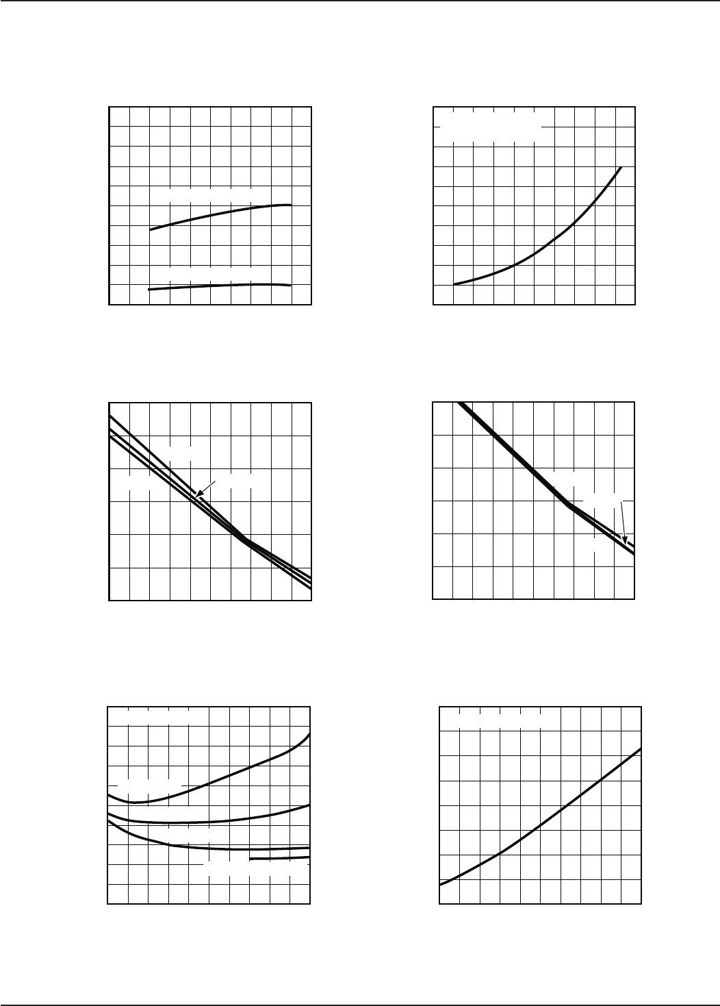
Typical Characteristic Curves
30
20
10
5
1000
10,000
CAPACITIVE LOAD (pF)
TIME (ns)
V = 18V
S
Fall Time vs. Capacitive Load
40
50
V = 12V
S
V = 5V
S
60
50
40
30
20
10
–60 –20 20 60 100
140
TEMPERATURE (°C)
TIME (ns)
D1
t
D2
t
Propagation Delay Time
vs.
Temperature
0 100 1000
10,000
CAPACITIVE LOAD (pF)
I – SUPPLY CURRENT (mA)
S
Supply Current vs. Capacitive Load
C = 2200 pF
L
V = 18V
S
84
70
56
42
28
14
0
500 kHz
200 kHz
20 kHz
V = 15V
S
60
50
40
30
20
10
0
DELAY TIME (ns)
4 6 8 10 12 14 16 18
SUPPLY VOLTAGE (V)
Delay Time vs. Supply Voltage
t
D2
t
D1
V = 12V
S
V = 5V
S
30
20
10
5
1000
10,000
CAPACITIVE LOAD (pF)
V = 18V
S
Rise Time vs. Capacitive Load
40
50
TIME (ns)
100
0
0 100 1000
10,000
FREQUENCY (kHz)
SUPPLY CURRENT (mA)
Supply Current vs. Frequency
10
1000
18V
10V
5V
C = 2200 pF
L
–60 –20 20 60 100
140
TEMPERATURE (°C)
5 7 9 11 13 15
V (V)
S
5 7 9 11 13 15
t
RISE
t
25
20
15
10
5
0
TIME (ns)
Rise and Fall Times vs. Temperature
C = 2200 pF
V = 18V
S
FALL
C = 2200 pF
L
60
50
40
30
20
10
0
TIME (ns)
Rise Time vs. Supply Voltage
C = 4700 pF
L
C = 10,000 pF
L
C = 2200 pF
L
TIME (ns)
Fall Time vs. Supply Voltage
C = 4700 pF
L
C = 10,000 pF
L
50
40
30
20
10
0
L
V (V)
S
3000
3000
M9999-072205 6 July 2005
MIC4420/4429 Micrel, Inc.
Typical Characteristic Curves (Cont.)
2.5
2
1.5
1
5 9 13
V (V)
S
Low-State Output Resistance
R ( )W
OUT
100 mA
50 mA
10 mA
7 11 15
1000
800
600
400
200
0
SUPPLY VOLTAGE (V)
900
800
700
600
500
400
–60 –20 20 60 100
140
TEMPERATURE (°C)
Quiescent Power Supply
Current vs. Temperature
LOGIC “1” INPUT
V = 18V
S
SUPPLY CURRENT (A)
0 4 8 12 16
20
SUPPLY CURRENT (A)
Quiescent Power Supply
Voltage vs. Supply Current
LOGIC “1” INPUT
5
4
3
2
5 9 13
V (V)
S
High-State Output Resistance
R ( )W
OUT
100 mA
50 mA
10 mA
7 11 15
200
160
120
80
40
0
DELAY (ns)
5 6 7 11 13
15
Effect of Input Amplitude
on Propagation Delay
LOAD = 2200 pF
INPUT 2.4V
INPUT 3.0V
INPUT 5.0V
INPUT 8V AND 10V
8 9 10 12 14
V (V)
S
2.0
1.5
1.0
0.5
0
CROSSOVER AREA (A•s) x 10
-8
5 6 7 11 13
15
Crossover Area vs. Supply Voltage
8 9 10 12 14
SUPPLY VOLTAGE V (V)
LOGIC “0” INPUT
PER TRANSITION
S

MIC4420YM

Mfr. #:
Manufacturer:
Microchip Technology / Micrel
Description:
Gate Drivers 6A Hi-Speed, Hi-Current Single MOSFET Driver
Lifecycle:
New from this manufacturer.
Delivery:
DHL FedEx Ups TNT EMS
Payment:
T/T Paypal Visa MoneyGram Western Union