July 2005 7 M9999-072205
MIC4420/4429 Micrel, Inc.
Applications Information
Supply Bypassing
Charging and discharging large capacitive loads quickly
requires large currents. For example, charging a 2500pF
load to 18V in 25ns requires a 1.8 A current from the device
power supply.
The MIC4420/4429 has double bonding on the supply pins,
the ground pins and output pins This reduces parasitic lead
inductance. Low inductance enables large currents to be
switched rapidly. It also reduces internal ringing that can
cause voltage breakdown when the driver is operated at
or near the maximum rated voltage.
Internal ringing can also cause output oscillation due to
feedback. This feedback is added to the input signal since
it is referenced to the same ground.
To guarantee low supply impedance over a wide frequency
range, a parallel capacitor combination is recommended for
supply bypassing. Low inductance ceramic disk capacitors
with short lead lengths (< 0.5 inch) should be used. A 1µF
low ESR film capacitor in parallel with two 0.1 µF low ESR
ceramic capacitors, (such as AVX RAM GUARD
®
), provides
adequate bypassing. Connect one ceramic capacitor di
-
rectly between pins 1 and 4. Connect the second ceramic
capacitor directly between pins 8 and 5.
Grounding
The high current capability of the MIC4420/4429 demands
careful PC board layout for best performance Since the
MIC4429 is an inverting driver, any ground lead impedance
will appear as negative feedback which can degrade switch
-
ing speed. Feedback is especially noticeable with slow-rise
time inputs. The MIC4429 input structure includes 300mV
of hysteresis to ensure clean transitions and freedom from
oscillation, but attention to layout is still recommended.
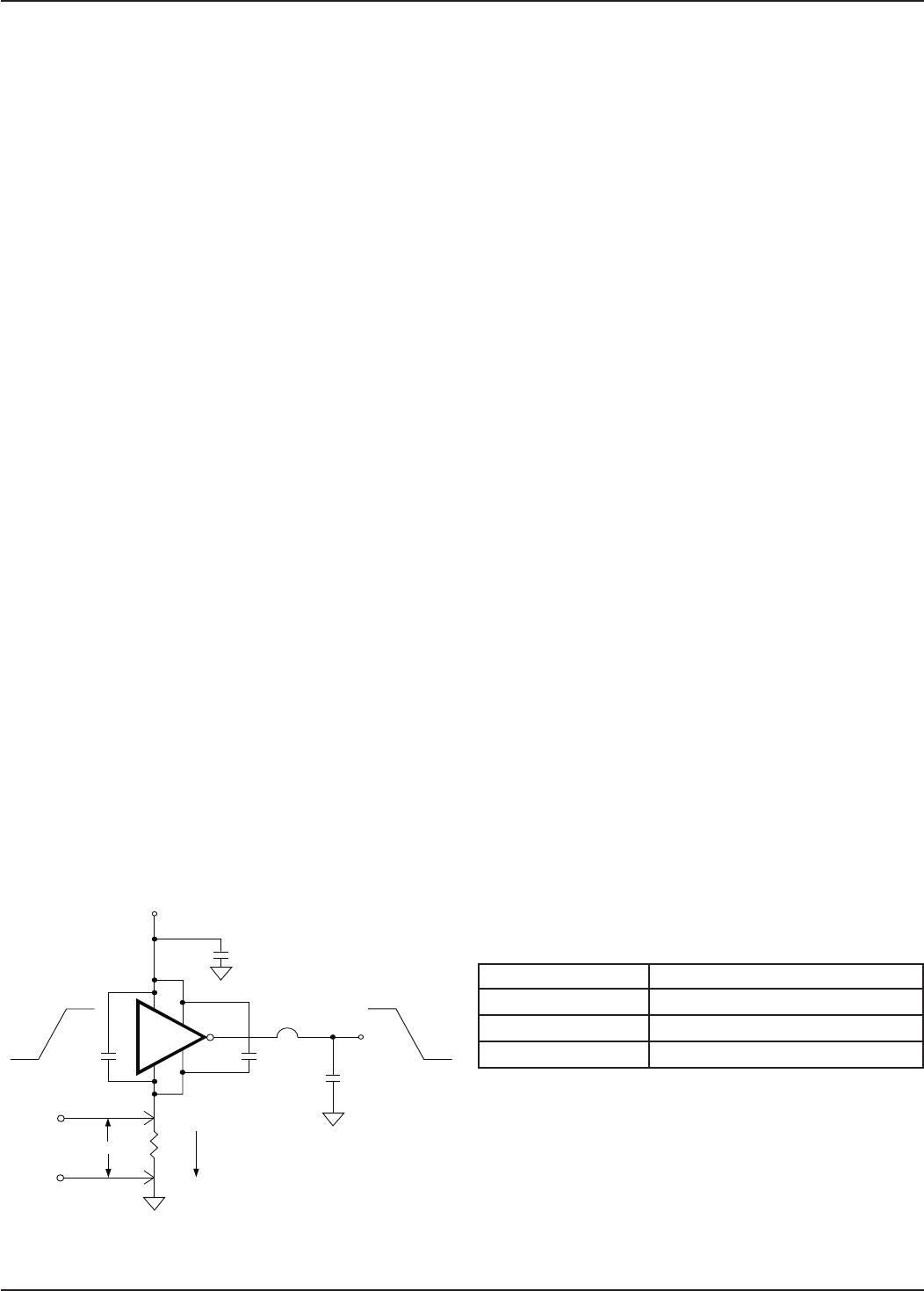
Figure 3 shows the feedback effect in detail. As the MIC4429
input begins to go positive, the output goes negative and
several amperes of current flow in the ground lead. As little
as 0.05Ω of PC trace resistance can produce hundreds of
millivolts at the MIC4429 ground pins. If the driving logic is
referenced to power ground, the effective logic input level
is reduced and oscillation may result.
To insure optimum performance, separate ground traces
should be provided for the logic and power connections.
Connecting the logic ground directly to the MIC4429 GND
pins will ensure full logic drive to the input and ensure fast
output switching. Both of the MIC4429 GND pins should,
however, still be connected to power ground.
Figure 3. Self-Contained Voltage Doubler
MIC4429
1µF
50V
MKS
2
UNITED C H E MCON SXE
0.1µF
WIMA
MKS
2
1
8
6,
7
5
4
0.1µF
50V
5.6 kΩ
560
+15
220 µF 50V
BYV 10 (x 2)
35 µF 50V
(x2) 1N4448
2
+
+
+
M9999-072205 8 July 2005
MIC4420/4429 Micrel, Inc.
Table 1: MIC4429 Maximum
Operating Frequency
V
S
Max Frequency
18V 500kHz
15V 700kHz
10V 1.6MHz
Conditions: 1. DIP Package (θ
JA
= 130°C/W)
2. T
A
= 25°C
3. C
L
= 2500pF
Input Stage
The input voltage level of the 4429 changes the quiescent
supply current. The N channel MOSFET input stage tran
-
sistor drives a 450µA current source load. With a logic “1”
input, the maximum quiescent supply current is 450µA.
Logic “0” input level signals reduce quiescent current to
55µA maximum.
The MIC4420/4429 input is designed to provide 300mV of
hysteresis. This provides clean transitions, reduces noise
sensitivity, and minimizes output stage current spiking when
changing states. Input voltage threshold level is approxi
-
mately 1.5V, making the device TTL compatible over the
4 .5V to 18V operating supply voltage range. Input current
is less than 10µA over this range.
The MIC4429 can be directly driven by the TL494,
SG1526/1527, SG1524, TSC170, MIC38HC42 and similar
switch mode power supply integrated circuits. By offloading
the power-driving duties to the MIC4420/4429, the power
supply controller can operate at lower dissipation. This can
improve performance and reliability.
The input can be greater than the
+
V
S
supply, however,
current will flow into the input lead. The propagation delay
for T
D2
will increase to as much as 400ns at room tem-
perature. The input currents can be as high as 30mA p-p
(6.4mA
RMS
) with the input, 6 V greater than the supply
voltage. No damage will occur to MIC4420/4429 however,
and it will not latch.
The input appears as a 7pF capacitance, and does not
change even if the input is driven from an AC source. Care
should be taken so that the input does not go more than 5
volts below the negative rail.
Power Dissipation
CMOS circuits usually permit the user to ignore power dis-
sipation. Logic families such as 4000 and 74C have outputs
which can only supply a few milliamperes of current, and
even shorting outputs to ground will not force enough cur
-
rent to destroy the device. The MIC4420/4429 on the other
hand, can source or sink several amperes and drive large
capacitive loads at high frequency. The package power
dissipation limit can easily be exceeded. Therefore, some
attention should be given to power dissipation when driving
low impedance loads and/or operating at high frequency.
The supply current vs frequency and supply current vs
capacitive load characteristic curves aid in determining
power dissipation calculations. Table 1 lists the maximum
safe operating frequency for several power supply volt
-
ages when driving a 2500pF load. More accurate power
dissipation figures can be obtained by summing the three
dissipation sources.
Given the power dissipation in the device, and the thermal
resistance of the package, junction operating temperature
for any ambient is easy to calculate. For example, the
thermal resistance of the 8-pin MSOP package, from the
data sheet, is 250°C/W. In a 25°C ambient, then, using a
maximum junction temperature of 150°C, this package will
dissipate 500mW.
Accurate power dissipation numbers can be obtained by
summing the three sources of power dissipation in the
device:
• Load Power Dissipation (P
L
)
• Quiescent power dissipation (P
Q
)
• Transition power dissipation (P
T
)
Calculation of load power dissipation differs depending on
whether the load is capacitive, resistive or inductive.
Resistive Load Power Dissipation
Dissipation caused by a resistive load can be calculated
as:
P
L
= I
2
R
O
D
where:
I = the current drawn by the load
R
O
= the output resistance of the driver when the output
is high, at the power supply voltage used. (See data
sheet)
D = fraction of time the load is conducting (duty cycle)
Figure 4. Switching Time Degradation Due to
Negative Feedback
MIC4429
1
8
6,
7
5
4
+18 V
0.1µF
0.1µF
TE K C U R R E N T
PROB E 6 302
2,500 pF
POL Y CAR BON ATE
5.0V
0 V
18 V
0 V
WIMA
MKS-2
1 µF
LOGIC
GROUND
POWER
GROUND
6 AMPS
300 mV
PC TRACE RESISTANCE = 0.05Ω
July 2005 9 M9999-072205
MIC4420/4429 Micrel, Inc.
where:
I
H
= quiescent current with input high
I
L
= quiescent current with input low
D = fraction of time input is high (duty cycle)
V
S
= power supply voltage
Transition Power Dissipation
Transition power is dissipated in the driver each time its
output changes state, because during the transition, for a
very brief interval, both the N- and P-channel MOSFETs in
the output totem-pole are ON simultaneously, and a cur
-
rent is conducted through them from V
+
S
to ground. The
transition power dissipation is approximately:
P
T
= 2 f V
S
(A•s)
where (A•s) is a time-current factor derived from the typical
characteristic curves.
Total power (P
D
) then, as previously described is:
P
D
= P
L
+ P
Q
+P
T
Definitions
C
L
= Load Capacitance in Farads.
D = Duty Cycle expressed as the fraction of time the
input to the driver is high.
f = Operating Frequency of the driver in Hertz
I
H
= Power supply current drawn by a driver when both
inputs are high and neither output is loaded.
I
L
= Power supply current drawn by a driver when both
inputs are low and neither output is loaded.
I
D
= Output current from a driver in Amps.
P
D
= Total power dissipated in a driver in Watts.
P
L
= Power dissipated in the driver due to the driver’s
load in Watts.
P
Q
= Power dissipated in a quiescent driver in
Watts.
P
T
= Power dissipated in a driver when the output
changes states (“shoot-through current”) in Watts.
NOTE: The “shoot-through” current from a dual
transition (once up, once down) for both drivers
is shown by the "Typical Characteristic Curve :
Crossover Area vs. Supply Voltage and is in am
-
pere-seconds. This figure must be multiplied by
the number of repetitions per second (frequency)
to find Watts.
R
O
= Output resistance of a driver in Ohms.
V
S
= Power supply voltage to the IC in Volts.
Capacitive Load Power Dissipation
Dissipation caused by a capacitive load is simply the en
-
ergy placed in, or removed from, the load capacitance by
the driver. The energy stored in a capacitor is described
by the equation:
E = 1/2 C V
2
As this energy is lost in the driver each time the load is
charged or discharged, for power dissipation calculations
the 1/2 is removed. This equation also shows that it is
good practice not to place more voltage on the capacitor
than is necessary, as dissipation increases as the square
of the voltage applied to the capacitor. For a driver with a
capacitive load:
P
L
= f C (V
S
)
2
where:
f = Operating Frequency
C = Load Capacitance
V
S
= Driver Supply Voltage
Inductive Load Power Dissipation
For inductive loads the situation is more complicated. For
the part of the cycle in which the driver is actively forcing
current into the inductor, the situation is the same as it is
in the resistive case:
P
L1
= I
2
R
O
D
However, in this instance the R
O
required may be either
the on resistance of the driver when its output is in the high
state, or its on resistance when the driver is in the low state,
depending on how the inductor is connected, and this is
still only half the story. For the part of the cycle when the
inductor is forcing current through the driver, dissipation is
best described as
P
L2
= I V
D
(1-D)
where V
D
is the forward drop of the clamp diode in the
driver (generally around 0.7V). The two parts of the load
dissipation must be summed in to produce P
L
P
L
= P
L1
+ P
L2
Quiescent Power Dissipation
Quiescent power dissipation (P
Q
, as described in the input
section) depends on whether the input is high or low. A low
input will result in a maximum current drain (per driver) of
≤0.2mA; a logic high will result in a current drain of ≤2.0mA.
Quiescent power can therefore be found from:
P
Q
= V
S
[D I
H
+ (1-D) I
L
]

MIC4420YM

Mfr. #:
Manufacturer:
Microchip Technology / Micrel
Description:
Gate Drivers 6A Hi-Speed, Hi-Current Single MOSFET Driver
Lifecycle:
New from this manufacturer.
Delivery:
DHL FedEx Ups TNT EMS
Payment:
T/T Paypal Visa MoneyGram Western Union