LTC2979
16
2979f
For more information www.linear.com/LTC2979
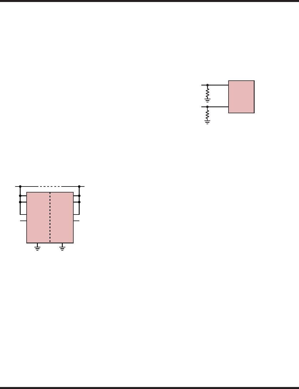
Figure 3. Undedicated Pull-Up Resistors
100k
100k
V
SENSEP
V
SENSEM
LTC2979
2979 F03
PCB ASSEMBLY AND LAYOUT SUGGESTIONS
Bypass Capacitor Placement
The LTC2979 requires 0.1µF bypass capacitors between
the V
DD33
pins and GND, the V
DD25
pins and GND, and
between the REFP and REFM pins. In order to be effective,
these capacitors should be made of high quality ceramic
dielectric such as X5R or X7R and be placed as close to
the chip as possible. The PCB layout should adhere to
good layout guidelines. A multilayer PCB that dedicates
a layer to power and ground is recommended. Low resis-
tance and low inductance power and ground connections
are important to minimize power supply noise and ensure
proper device operation.
DESIGN CHECKLIST
I
2
C
n
Each half of the LTC2979 must be configured for a
unique address. Unique hardware ASELn values are
recommended for simplest in-system programming.
n
The address select pins (ASEL
n
) are tri-level; Check
Table 1 of the LTC2977 data sheet.
n
Check addresses for collision with other devices on the
bus and any global addresses.
APPLICATIONS INFORMATION
OVERVIEW
The LTC2979 is a digital power system manager that
is capable of sequencing, margining, trimming, super-
vising output voltage for OV/UV conditions, providing
fault management, and voltage readback for sixteen
DC/DC converters. Input voltage and LTC2979 junction
temperature readback are also available. Odd numbered
channels can be configured to read back current sense
resistor voltages. Multiple LTC2979s can be synchronized
to operate in unison using the SHARE_CLK, FAULTB and
CONTROL pins. The LTC2979 utilizes a PMBus compliant
interface and command set.
POWERING THE LTC2979
The LTC2979 is powered from a 3.13V to 3.47V supply
connected to the V
DD33
pins. Tie all the V
DD33
pins on each
half of the device together. See Figure 2. Separate 3.3V
supplies can be used for V
DD33(A)
and V
DD33(B)
.
Unused ADC Sense Inputs
Connect all unused ADC sense inputs (V
SENSEPn
or
V
SENSEMn
) to GND. In a system where the inputs are con-
nected to removable cards and may be left floating in
certain situations, connect the inputs to GND using 100k
resistors, as shown in Figure 3.
Figure 2. Powering LTC2979 from a 3.3V Supply
V
DD33
V
DD33
V
DD33
V
DD25
V
DD33
V
DD33
V
DD33
V
DD25
LTC2979*
DEVICE A
3.3V
GND
*SOME DETAILS
OMITTED FOR CLARITY
2979 F02
3.3V
LTC2979*
DEVICE B
GND
APPLICATION CIRCUITS
V
IN
Sense
Voltages other than V
IN
can be monitored and supervised
using the V
IN_SNS
pins. Each V
IN_SNS
pin has a calibrated
internal divider allowing it to directly sense voltages up
to 15V.