LTC1646
1
1646fa
CompactPCI Bus Removable Boards
Allows Safe Board Insertion and Removal from a
Live, CompactPCI
TM
Bus
Controls 3.3V and/or 5V Supplies
Programmable Foldback Current Limit During
Power-Up
Dual Level Circuit Breakers Protect Supplies from
Overcurrent and Short-Circuit Faults
LOCAL_PCI_RST# Logic On-Chip
PRECHARGE Output Biases I/O Pins During Card
Insertion and Extraction
User Programmable Supply Voltage Power-Up Rate
15V High Side Drive for External N-Channel
MOSFETS
PWRGD, RESETOUT and FAULT Outputs
CompactPCI Dual
Hot Swap Controller
The LTC
®
1646 is a Hot Swap
TM
controller that allows a
board to be safely inserted and removed from a live
CompactPCI bus slot. Two external N-Channel transistors
control the 3.3V and 5V supplies. The supplies can be
ramped-up in current limit or a programmable rate. Elec-
tronic circuit breakers protect both supplies against
overcurrent fault conditions. The PWRGD output indicates
when all of the supply voltages are within tolerance. The
OFF/ON pin is used to cycle the board power or reset the
circuit breaker. The PRECHARGE output can be used to
bias the bus I/O pins during card insertion and extraction.
PCI_RST# is logically combined on-chip with HEALTHY#
in order to generate LOCAL_PCI_RST# which can be used
to reset the CPCI card logic if either of the supply voltages
is not within tolerance.
The LTC1646 is available in the 16-pin narrow SSOP
package.
Figure 1
MMBT2222A
4.7nF
18
18
12
10
2.7
1.8
R3
10
3k
R4
10
3k
1k
R1
0.005, 1%
R2
0.007
1%
1k
R5
1k, 5%
10k
10k
3k
1.2k
3V
IN
PRECHARGE OUT
1V ±10%
I
OUT
= ± 55mA
3V
IN
3V
IN
3V
SENSE
5V
SENSE
3V
OUT
3V
OUT
5V
OUT
3.3V
5V
IN
5V
IN
5V
RESET#
I/O
PCI
BRIDGE
(21154)
DATA BUS
DATA BUS
V(I/O)
V(I/O)
0.1µF 0.1µF
0.1µF
C1
0.01µF
Q2
IRF7413
Q1
IRF7413
LOCAL_PCI_RST#
5V
5A
3.3V
7.6A
GATE
GND PRECHARGE DRIVE
RESETOUT
TIMER
OFF/ON
FAULT
PWRGD
RESETIN
LTC1646
15
891071211 5
2
1
613 14
3
4
16
BD_SEL#
HEALTHY#
PCI_RST#
1646 F01
DATA LINE EXAMPLE
COMPACT PCI
BACKPLANE
CONNECTOR
(MALE)
COMPACT PCI
CIRCUIT CARD
CONNECTOR
(FEMALE)
5V
LONG 5V
3.3V
LONG 3.3V
GROUND
I/O PIN 1
Z1, Z2: BZX84C6V2
Z2
Z1
APPLICATIO S
U
FEATURES
TYPICAL APPLICATIO
U
DESCRIPTIO
U
, LTC and LT are registered trademarks of Linear Technology Corporation.
Hot Swap is a trademark of Linear Technology Corporation.
All other trademarks are the property of their respective owners.
LTC1646
2
1646fa
SYMBOL PARAMETER CONDITIONS MIN TYP MAX UNITS
I
DD
V
5VIN
Supply Current OFF/ON = 0V 1.5 4 mA
V
LKO
Undervoltage Lockout 5V
IN
2.3 2.50 2.7 V
3V
IN
2.3 2.55 2.7 V
V
FB
Foldback Current Limit Voltage V
FB
= (V
5VIN
–V
5VSENSE
), V
5VOUT
= 0V, TIMER = 0V 15 20 30 mV
V
FB
= (V
5VIN
– V
5VSENSE
), V
5VOUT
= 4V, TIMER = 0V 50 55 65 mV
V
FB
= (V
3VIN
– V
3VSENSE
), V
3VOUT
= 0V, TIMER = 0V 15 20 30 mV
V
FB
= (V
3VIN
– V
3VSENSE
), V
3VOUT
= 2V, TIMER = 0V 50 55 65 mV
V
CB
Circuit Breaker Trip Voltage V
CB
= (V
5VIN
– V
5VSENSE
), V
5VOUT
= 5V, TIMER Open 50 56 65 mV
V
CB
= (V
3VIN
– V
3VSENSE
), V
3VOUT
= 3.3V, TIMER Open 50 56 65 mV
t
OC
Overcurrent Fault Response Time (V
5VIN
– V
5VSENSE
) = 100mV, TIMER Open 10 21 30 µs
(V
3VIN
– V
3VSENSE
) = 100mV, TIMER Open 10 21 30 µs
t
SS
Short-Circuit Fault Response Time (V
5VIN
– V
5VSENSE
) = 200mV, TIMER Open 0.145 1 µs
(V
3VIN
– V
3VSENSE
) = 200mV, TIMER Open 0.145 1 µs
I
CP
GATE Pin Output Current OFF/ON = 0V, V
GATE
= 0V, TIMER = 0V –18 –13 –8 µA
OFF/ON = 5V, V
GATE
= 5V, TIMER = 0V 80 200 300 µA
OFF/ON = 0V, V
GATE
= 5V, FAULT = 0V, TIMER Open 4712mA
V
GATE
External Gate Voltage OFF/ON = 0V, I
GATE
= –1µA 12 15 16 V
(GATE to GND) OFF/ON = 0V, V
5VIN
= 3.3V, I
GATE
= –1µA 11 13 15 V
V
TH
Power Good Threshold Voltage 3V
OUT
2.8 2.9 3.0 V
5V
OUT
4.5 4.65 4.75 V
V
3VONLY
No 5V Input Mode Window Voltage V
3VONLY
= V
5VIN
– V
3VIN
, V
5VOUT
= V
3VOUT
= 3.3V 50 120 200 mV
V
IL
Input Low Voltage OFF/ON, RESETIN, FAULT 0.8 V
ORDER PART NUMBER
T
JMAX
= 125°C, θ
JA
= 135°C/W
Consult LTC Marketing for parts specified with wider operating temperature ranges.
LTC1646CGN
LTC1646IGN
ABSOLUTE AXI U RATI GS
W
WW
U
PACKAGE/ORDER I FOR ATIO
UUW
(Note 1)
ELECTRICAL CHARACTERISTICS
The denotes the specifications which apply over the full operating
temperature range, otherwise specifications are at T
A
= 25°C. V
5VIN
= 5V and V
3VIN
= 3.3V unless otherwise noted.
Supply Voltages: 5V
IN
, 3V
IN
...............................................
10V
Input Voltages: (Pins 15, 16) ..................... 0.3V to 10V
Output Voltages: (Pins 1, 3, 4) .................. 0.3V to 10V
Analog Voltages and Currents:
(Pin 9) .................................... 0.3V to (3V
IN
+ 0.3V)
(Pins 2, 5, 7, 11, 13, 14) ........ 0.3V to (5V
IN
+ 0.3V)
(Pin 10) .......................................................... ±20mA
Operating Temperature Range:
LTC1646C ............................................... 0°C to 70°C
LTC1646I.............................................40°C to 85°C
Storage Temperature Range ..................65°C to 150°C
Lead Temperature (Soldering, 10 sec).................. 300°C
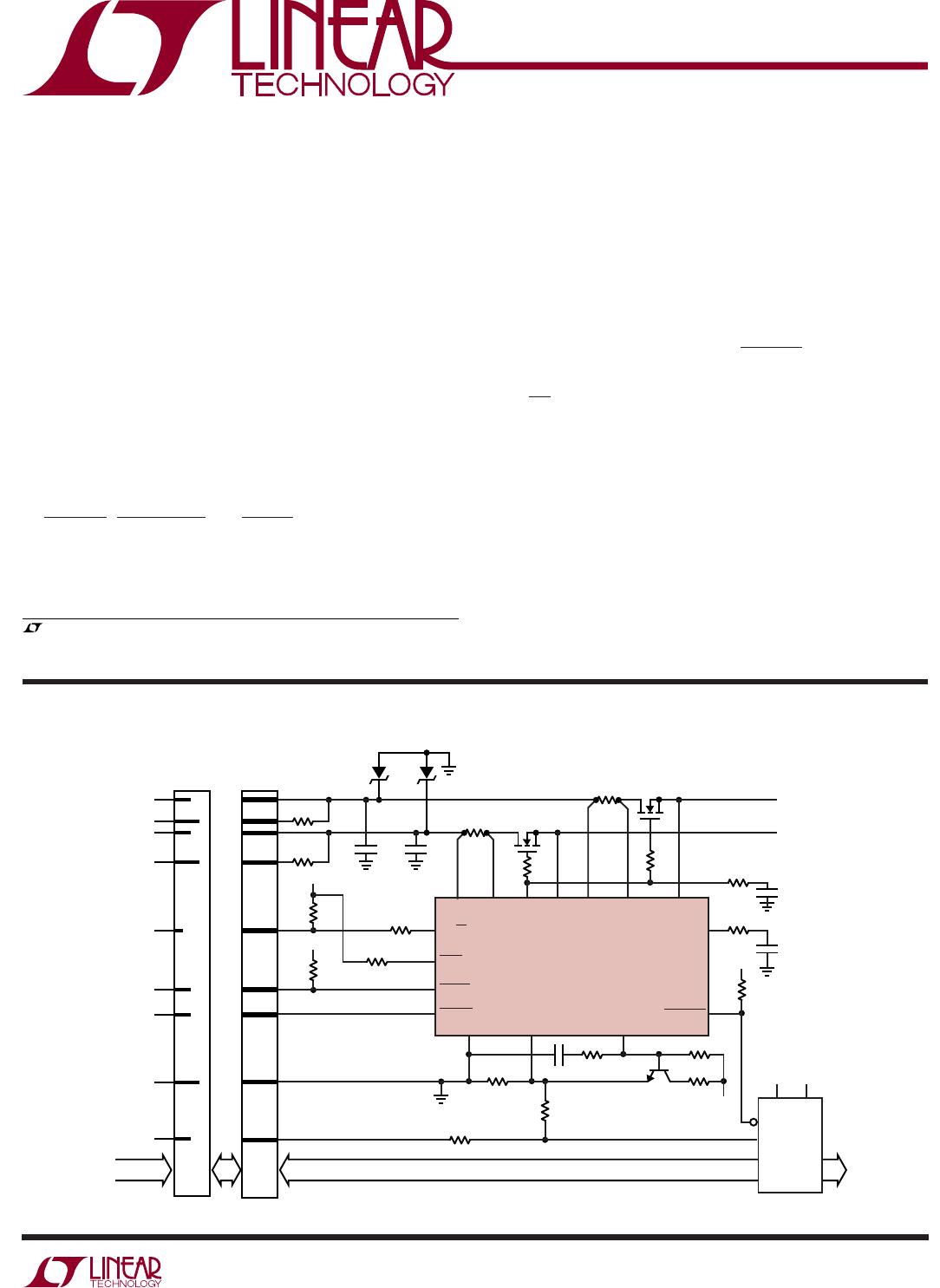
TOP VIEW
GN PACKAGE
16-LEAD PLASTIC SSOP
1
2
3
4
5
6
7
8
16
15
14
13
12
11
10
9
RESETOUT
TIMER
FAULT
PWRGD
5V
OUT
GND
3V
OUT
3V
IN
RESETIN
OFF/ON
DRIVE
PRECHARGE
5V
IN
5V
SENSE
GATE
3V
SENSE
GN PART MARKING
1646
1646I
Order Options Tape and Reel: Add #TR
Lead Free: Add #PBF Lead Free Tape and Reel: Add #TRPBF
Lead Free Part Marking: http://www.linear.com/leadfree/
LTC1646
3
1646fa
SYMBOL PARAMETER CONDITIONS MIN TYP MAX UNITS
V
IH
Input High Voltage OFF/ON, RESETIN, FAULT 2V
V
TIMER
TIMER Threshold Voltage V
TIMER
, FAULT = 0V 1.15 1.25 1.35 V
I
IN
OFF/ON Input Current OFF/ON = 5V ±0.08 ±10 µA
OFF/ON = 0V
±0.08 ±10 µA
RESETIN Input Current RESETIN = 5V ±0.08 ±10 µA
RESETIN = 0V
±0.08 ±10 µA
5V
SENSE
Input Current 5V
SENSE
= 5V, 5V
OUT
= 0V 66 100 µA
3V
SENSE
Input Current 3V
SENSE
= 3.3V, 3V
OUT
= 0V 66 100 µA
3V
IN
Input Current 3V
IN
= 3.3V 460 1000 µA
5V
OUT
Input Current 5V
OUT
= 5V, OFF/ON = 0V 0.9 1.5 mA
3V
OUT
Input Current 3V
OUT
= 3.3V, OFF/ON = 0V 0.9 1.5 mA
I
TIMER
TIMER Pin Current OFF/ON = 0V, V
TIMER
= 0V –7 –5 –3 µA
OFF/ON = 5V, V
TIMER
= 5V 6.6 mA
R
DIS
5V
OUT
Discharge Impedance OFF/ON = 5V 120 220
3V
OUT
Discharge Impedance OFF/ON = 5V 120 220
V
OL
Output Low Voltage FAULT, PWRGD, RESETOUT, I = 2mA 0.25 0.4 V
V
PXG
PRECHARGE Reference Voltage V
PRECHARGE
, V
5VIN
= 5V and 3.3V 0.90 1.00 1.10 V
ELECTRICAL CHARACTERISTICS
The denotes the specifications which apply over the full operating
temperature range, otherwise specifications are at T
A
= 25°C. V
5VIN
= 5V and V
3VIN
= 3.3V unless otherwise noted.
Note 1: Absolute Maximum Ratings are those values beyond which the life
of a device may be impaired.
Note 2: All currents into device pins are positive; all currents out of device
pins are negative. All voltages are referenced to ground unless otherwise
specified.
TYPICAL PERFOR A CE CHARACTERISTICS
UW
5V Current Foldback Profile 3.3V Current Foldback Profile
OUTPUT VOLTAGE (V)
0
OUTPUT CURRENT (A)
2
4
5
1646 G01
13
12
11
10
9
8
7
6
5
4
3
2
1
0
R
SENSE
= 0.007
1646 G02
12
11
10
9
8
7
6
5
4
3
2
1
0
OUTPUT VOLTAGE (V)
0
OUTPUT CURRENT (A)
2
4
5
13
R
SENSE
= 0.005
50 25 0 25 50 75 100
TEMPERATURE (°C)
SUPPLY CURRENT (mA)
1646 G03
1.8
1.7
1.6
1.5
1.4
1.3
1.2
1.1
1.0
5V
IN
Supply Current vs
Temperature

LTC1646IGN#PBF

Mfr. #:
Manufacturer:
Analog Devices Inc.
Description:
Hot Swap Voltage Controllers CompactPCI 2x Hot Swap Cntr
Lifecycle:
New from this manufacturer.
Delivery:
DHL FedEx Ups TNT EMS
Payment:
T/T Paypal Visa MoneyGram Western Union