LTC1646
14
1646fa
APPLICATIO S I FOR ATIO
WUUU
(RTOL = ±1%, ±2% or ±5%) and standard sense resistor
values. Equation 7 can be used to calculate the nominal
value from the maximum value found by Equation 6:
R
R
RTOL
SENSE NOM
SENSE MAX
()
()
=
+
⎛
⎝
⎜
⎞
⎠
⎟
1
100
(7)
Often, the result of Equation 7 may not yield a standard
sense resistor value. In this case, two sense resistors with
the same RTOL can be connected in parallel to yield
R
SENSE(NOM)
.
The last step requires calculating a new value for
I
TRIP(MAX)
(I
TRIP(MAX, NEW)
) based on a minimum value for
R
SENSE
(R
SENSE(MIN)
) and the upper limit for the circuit
breaker threshold, V
CB(MAX)
. Should the calculated value
for I
TRIP(MAX, NEW)
be much greater than the design value
for I
TRIP(MAX)
, a larger sense resistor value should be
selected and the process repeated. The new value for
I
TRIP(MAX, NEW)
is given by Equation 8:
I
V
R
where R R
RTOL
TRIP MAX NEW
CB MAX
SENSE MIN
SENSE MIN SENSE NOM
(,)
()
()
() ( )
()
•–
=
=
⎛
⎝
⎜
⎞
⎠
⎟
⎡
⎣
⎢
⎤
⎦
⎥
8
1
100
Example
: A 5V supply exhibits a nominal 5A load with a
maximum load current of 6.8A (I
LOAD(MAX)
= 6.8A), and
sense resistors with ±5% RTOL will be used. According to
Equation 6, V
CB(MIN)
= 50mV and R
SENSE(MAX)
is given by:
R
V
I
mV
A
SENSE MAX
CB MIN
TRIP MAX
()
()
()
.
.===Ω
50
68
0 0074
The nominal sense resistor value is (Equation 7):
R
R
RTOL
SENSE NOM
SENSE MAX
()
()
.
.=
+
⎛
⎝
⎜
⎞
⎠
⎟
=
Ω
+
⎛
⎝
⎜
⎞
⎠
⎟
= Ω
1
100
0 0074
1
5
100
0 007
And the new current-limit trip point is Equation 8:
I
V
R
V
R
RTOL
mV
A
TRIP MAX NEW
CB MAX
SENSE MIN
CB MAX
SENSE N M
(,)
()
()
()
()
•–
.
.
==
⎛
⎝
⎜
⎞
⎠
⎟
⎡
⎣
⎢
⎤
⎦
⎥
==
0
1
100
65
0 0065
98
Since I
TRIP(MAX, NEW)
> I
LOAD(MAX)
, a larger value for
R
SENSE
should be selected and the process repeated again
to lower I
TRIP(MAX, NEW)
without substantially affecting
I
LOAD(MAX)
.
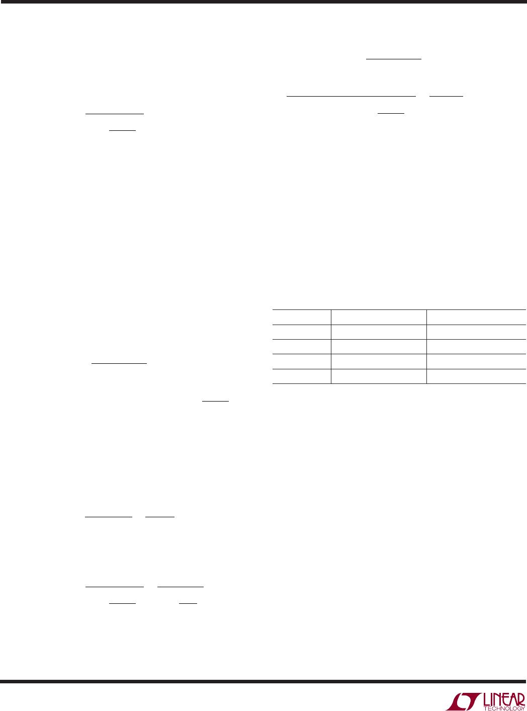
Output Voltage Monitor
The status of both 5V and 3.3V output voltages is moni-
tored by the power good function. In addition, the PCI_RST#
signal is logically combined on-chip with the HEALTHY#
signal to create LOCAL_PCI_RST# (see Table 4).
Table 4. LOCAL_PCI_RST# Truth Table
PCI_RST# HEALTHY# LOCAL_PCI_RST#
LO LO LO
LO HI LO
HI LO HI
HI HI LO
If either of the output voltages drop below the power good
threshold for more than 50µs, the HEALTHY# signal will be
pulled high and the LOCAL_PCI_RST# signal will be pulled
low.
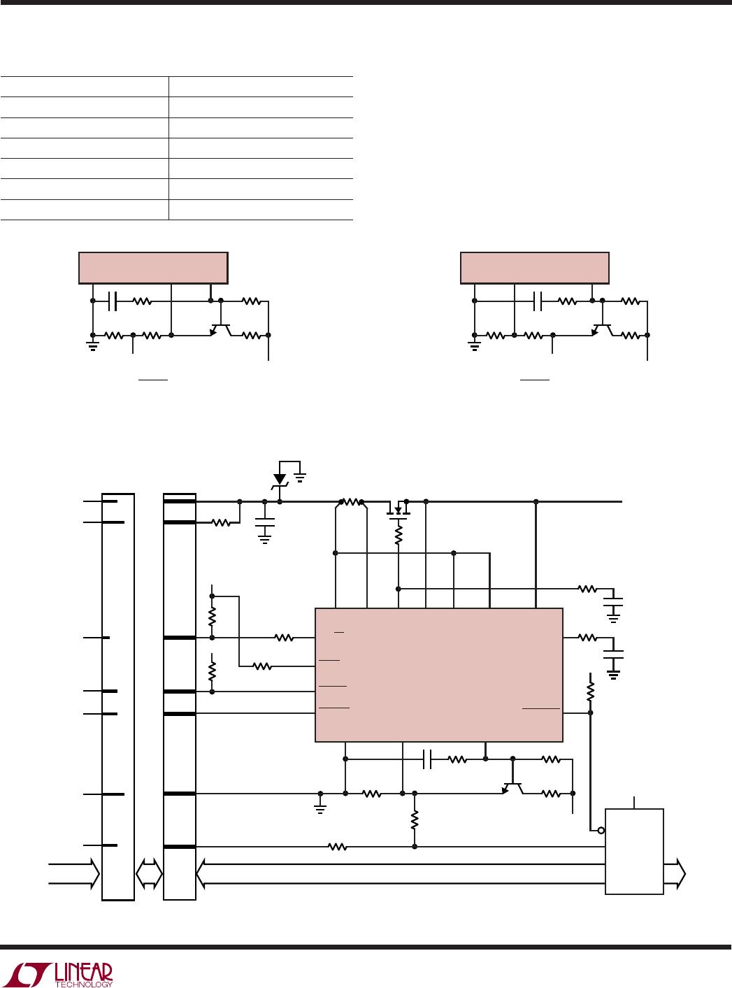
Precharge
The PRECHARGE input and DRIVE output pins are in-
tended for use in generating the 1V precharge voltage that
is used to bias the bus I/O connector pins during board
insertion. The LTC1646 is also capable of generating
precharge voltages other than 1V. Figure 8 shows a circuit
that can be used in applications requiring a precharge
voltage less than 1V. The circuit in Figure 9 can be used for
applications that need precharge voltages greater than 1V.
Table 5 lists suggested resistor values for R1 and R2 vs
precharge voltage for the application circuits shown in
Figures 8 and 9.