6
82C54
Functional Description
General
The 82C54 is a programmable interval timer/counter
designed for use with microcomputer systems. It is a general
purpose, multi-timing element that can be treated as an
array of I/O ports in the system software.
The 82C54 solves one of the most common problems in any
microcomputer system, the generation of accurate time
delays under software control. Instead of setting up timing
loops in software, the programmer configures the 82C54 to
match his requirements and programs one of the counters
for the desired delay. After the desired delay, the 82C54 will
interrupt the CPU. Software overhead is minimal and
variable length delays can easily be accommodated.
Some of the other computer/timer functions common to
microcomputers which can be implemented with the 82C54
are:
• Real time clock
• Event counter
• Digital one-shot
• Programmable rate generator
• Square wave generator
• Binary rate multiplier
• Complex waveform generator
• Complex motor controller
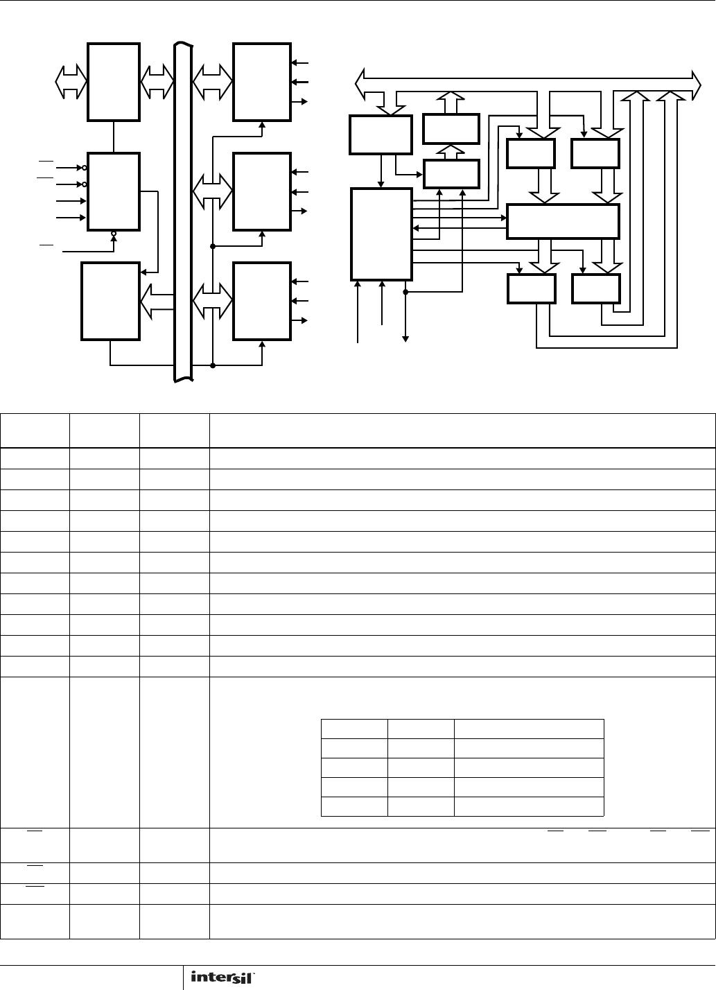
Data Bus Buffer
This three-state, bi-directional, 8-bit buffer is used to
interface the 82C54 to the system bus (see Figure 1).
Read/Write Logic
The Read/Write Logic accepts inputs from the system bus and
generates control signals for the other functional blocks of the
82C54. A1 and A0 select one of the three counters or the
Control Word Register to be read from/written into. A “low” on
the RD
input tells the 82C54 that the CPU is reading one of the
counters. A “low” on the WR
input tells the 82C54 that the CPU
is writing either a Control Word or an initial count. Both RD
and
WR
are qualified by CS; RD and WR are ignored unless the
82C54 has been selected by holding CS
low.
Control Word Register
The Control Word Register (Figure 2) is selected by the
Read/Write Logic when A1, A0 = 11. If the CPU then does a
write operation to the 82C54, the data is stored in the Control
Word Register and is interpreted as a Control Word used to
define the Counter operation.
The Control Word Register can only be written to; status
information is available with the Read-Back Command.
Counter 0, Counter 1, Counter 2
These three functional blocks are identical in operation, so
only a single Counter will be described. The internal block
diagram of a signal counter is shown in Figure 3. The
counters are fully independent. Each Counter may operate
in a different Mode.
The Control Word Register is shown in the figure; it is not
part of the Counter itself, but its contents determine how the
Counter operates.
CONTROL
WORD
REGISTER
COUNTER
2
COUNTER
1
COUNTER
0
INTERNAL BUS
OUT 2
GATE 2
CLK 2
OUT 1
GATE 1
CLK 1
OUT 0
GATE 0
CLK 0
WR
RD
D
7
- D
0
A
0
A
1
CS
FIGURE 1. DATA BUS BUFFER AND READ/WRITE LOGIC
FUNCTIONS
8
DATA/
BUS
BUFFER
READ/
WRITE
LOGIC
READ/
WRITE
LOGIC
DATA/
BUS
BUFFER
INTERNAL BUS
OUT 2
GATE 2
CLK 2
OUT 1
GATE 1
CLK 1
OUT 0
GATE 0
CLK 0
WR
RD
D
7
- D
0
A
0
A
1
CS
FIGURE 2. CONTROL WORD REGISTER AND COUNTER
FUNCTIONS
8
CONTROL
WORD
REGISTER
COUNTER
2
COUNTER
1
COUNTER
0