AD8625/AD8626/AD8627 Data Sheet
Rev. F | Page 4 of 20
@V
S
= ±13 V; V
CM
= 0 V; T
A
= 25°C, unless otherwise noted.
Table 2.
Parameter Symbol Conditions Min Typ Max Unit
INPUT CHARACTERISTICS
Offset Voltage V
OS
0.35 0.75 mV
40°C < T
A
< +85°C 1.35 mV
Input Bias Current
B
0.25
1
pA
40°C < T
A
< +85°C 60 pA
Input Offset Current I
OS
0.5 pA
40°C < T
A
< +85°C 25 pA
Input Voltage Range 13 +11 V
Common-Mode Rejection Ratio
V
CM
= 13 V to +10 V
76
105
dB
Large Signal Voltage Gain A
VO
R
L
= 10 kΩ, V
O
= 11 V to +11 V 150 310 V/mV
Offset Voltage Drift ∆V
OS
/∆T 40°C < T
A
< +85°C 2.5 µV/°C
OUTPUT CHARACTERISTICS
Output Voltage High V
OH
+12.92 V
V
OH
I
L
= 2 mA, 40°C < T
A
< +85°C +12.91 V
Output Voltage Low V
OL
12.92 V
V
OL
I
L
= 2 mA, 40°C < T
A
< +85°C 12.91 V
Output Current I
OUT
±15 mA
POWER SUPPLY
Power-Supply Rejection Ratio PSRR V
S
= ±2.5 V to ±13 V 80 104 dB
Supply Current/Amplifier I
SY
710 850 µA
40°C < T
A
< +85°C 900 µA
DYNAMIC PERFORMANCE
Slew Rate SR 5 V/µs
Gain Bandwidth Product GBP 5 MHz
Phase Margin Ø
M
60 Degrees
NOISE PERFORMANCE
Voltage Noise e
n
p-p 0.1 Hz to 10 Hz 2.5 µV p-p
Voltage Noise Density e
n
f = 1 kHz 16 nV/√Hz
Current Noise Density i
n
f = 1 kHz 0.5 fA/√Hz
Channel Separation C
s
f = 1 kHz 105 dB
Data Sheet AD8625/AD8626/AD8627
Rev. F | Page 5 of 20
ABSOLUTE MAXIMUM RATINGS
Table 3.
Parameter Ratings
Supply Voltage 27 V
Input Voltage V
S–
to V
S+
Differential Input Voltage ± Supply Voltage
Output Short-Circuit Duration Indefinite
Storage Temperature Range, R Package
65°C to +125°C
Operating Temperature Range
40°C to +85°C
Junction Temperature Range, R Package
65°C to +150°C
Lead Temperature Range (Soldering, 60 sec)
300°C
Stresses above those listed under Absolute Maximum Ratings
may cause permanent damage to the device. This is a stress
rating only; functional operation of the device at these or any
other conditions above those indicated in the operational
section of this specification is not implied. Exposure to absolute
maximum rating conditions for extended periods may affect
device reliability.
θ
JA
is specified for worst-case conditions when devices are
soldered in circuit boards for surface-mount packages.
Table 4.
Package Type θ
JA
θ
JC
Unit
5-Lead SC70 (KS) 376 126 °C/W
8-Lead MSOP (RM) 210 45 °C/W
8-Lead SOIC (R) 158 43 °C/W
14-Lead SOIC (R) 120 36 °C/W
14-Lead TSSOP (RU) 180 35 °C/W
ESD CAUTION
AD8625/AD8626/AD8627 Data Sheet
Rev. F | Page 6 of 20
TYPICAL PERFORMANCE CHARACTERISTICS
03023-002
VOLTAGE (
µ
V)
25
20
0
–600 –400
NUMBER OF AMPLIFIERS
–200
0
200 400
600
15
10
5
V
SY
=
±
12V
T
A
= 25
°
C
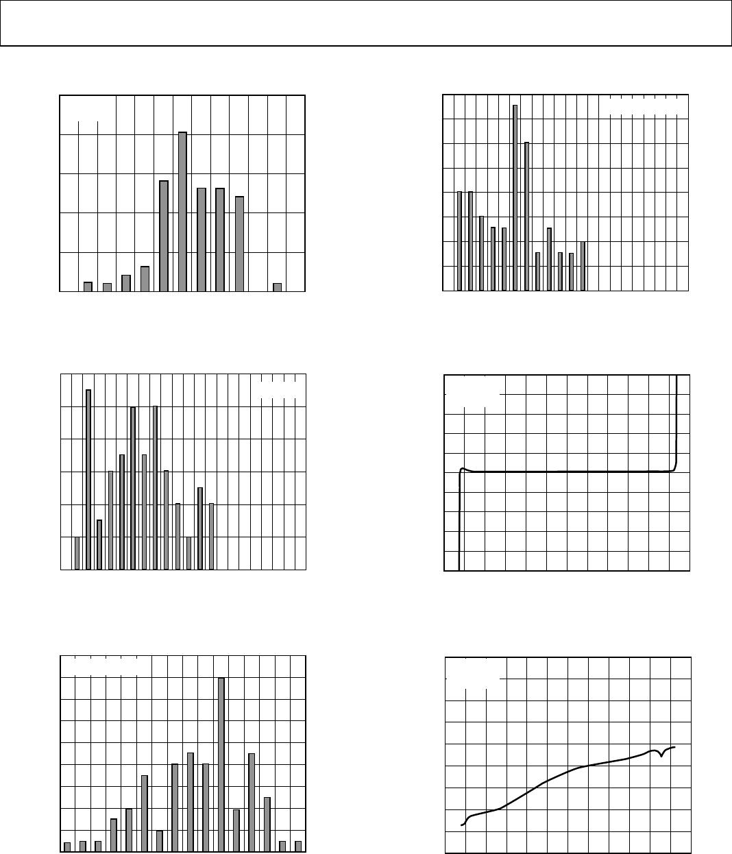
Figure 2. Input Offset Voltage
OFFSET VOLTAGE (
µ
V/
°
C)
12
0
0 1 2 3 4 5 6 7 8 9 10
03023-003
NUMBER OF AMPLIFIERS
6
4
2
8
10
V
SY
=
±
13V
Figure 3. Offset Voltage Drift
VOLTAGE (
µ
V)
18
16
14
12
10
8
6
4
2
0
400 –300 –200 –100 0 100 200 300
03023-004
NUMBER OF AMPLIFIERS
V
SY
= +3.5V/–1.5V
Figure 4. Input Offset Voltage
OFFSET VOLTAGE (
µ
V/
°
C)
16
14
12
10
8
6
4
2
0
0
1
2 3 4 5 6 7 8 9 10
03023-005
NUMBER OF AMPLIFIERS
V
SY
= +3.5V/–1.5V
Figure 5. Offset Voltage Drift
V
CM
(V)
50
–50
–40
–30
20
–10
0
10
20
30
40
15.0–12.5
–10.0 –
7.5 –5.0 –2.5 0 2.5 5.0 7.5 10.0 12.5 15.0
03023-006
INPUT BIAS CURRENT (pA)
V
SY
=
±
13V
T
A
= 25
°
C
Figure 6. Input Bias Current vs. V
CM
V
CM
(V)
–0.9
0
–0.1
–0.2
–0.3
–0.4
–0.5
–0.6
–0.7
–0.8
–15.0–12.5–10.0 –7.5
5.0 –2.5 0 2.5 5.0 7.5 10.0 12.5 15.0
03023-007
INPUT BIAS CURRENT (pA)
V
SY
=
±
13V
T
A
= 25
°
C
Figure 7. Input Bias Current vs. V
CM

AD8625ARZ-REEL

Mfr. #:
Manufacturer:
Analog Devices Inc.
Description:
Precision Amplifiers Prec Low Pwr JFET SGL-Supply
Lifecycle:
New from this manufacturer.
Delivery:
DHL FedEx Ups TNT EMS
Payment:
T/T Paypal Visa MoneyGram Western Union