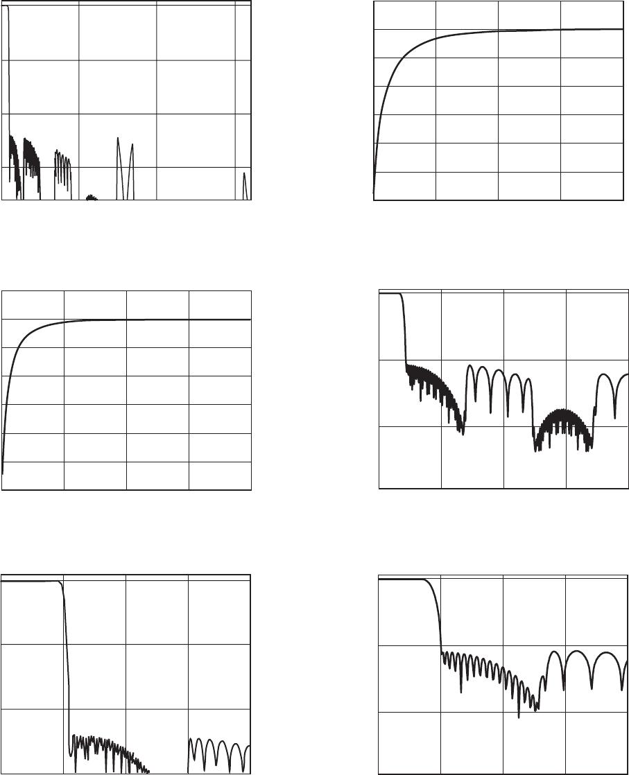
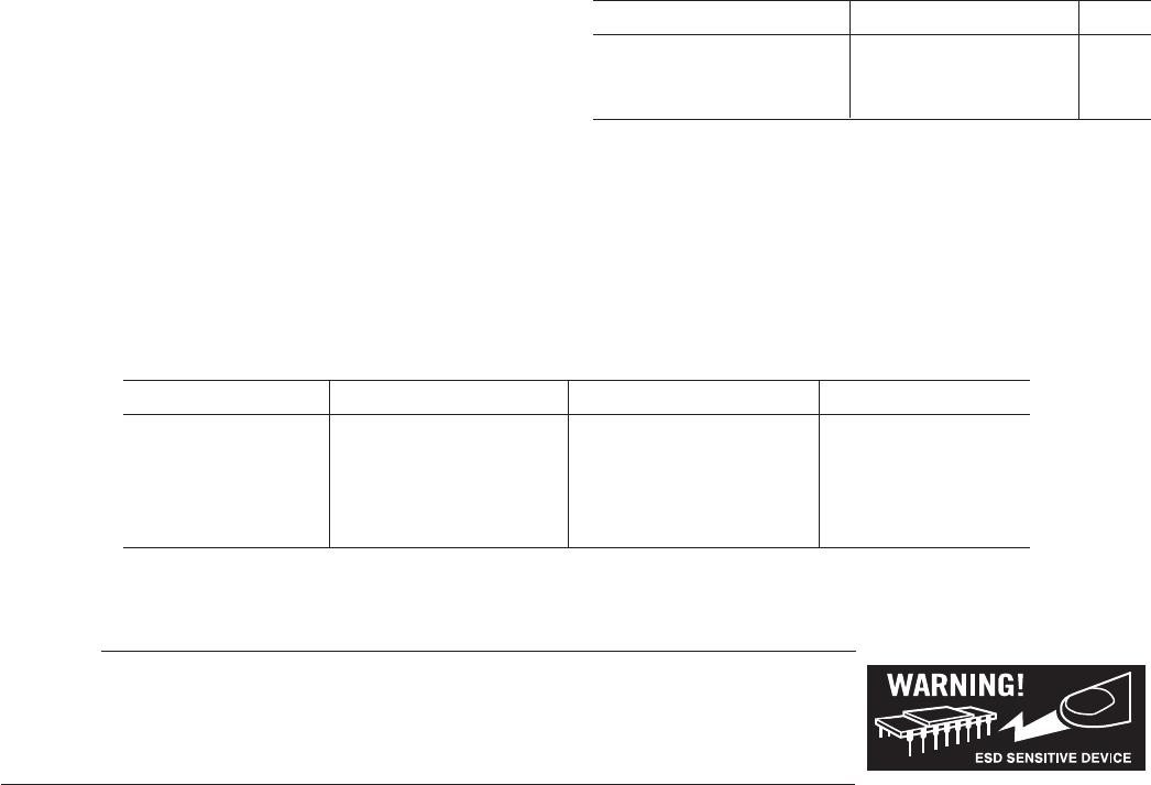
REV. A
AD1838A
–6–
ORDERING GUIDE
Model Temperature Range Package Description Package Option
AD1838AAS –40°C to +85°C 52-Lead MQFP S-52-1
AD1838AAS-REEL –40°C to +85°C 52-Lead MQFP S-52-1
AD1838AASZ* –40°C to +85°C 52-Lead MQFP S-52-1
AD1838AASZ-REEL* –40°C to +85°C 52-Lead MQFP S-52-1
EVAL-AD1838AEB –40°C to +85°C 52-Lead MQFP S-52-1
*Z = Pb-free part.
TEMPERATURE RANGE
Parameter Min Typ Max Unit
Specifications Guaranteed 25 °C
Functionality Guaranteed –40 +85 °C
Storage –65 +150 °C
ABSOLUTE MAXIMUM RATINGS*
(T
A
= 25°C, unless otherwise noted.)
AVDD, DVDD, ODVDD to AGND, DGND
. . . . . . . . . . . . . . . . . . . . . . . . . . . . . . . . . . . . –0.3 V to +6 V
AGND to DGND . . . . . . . . . . . . . . . . . . . . –0.3 V to +0.3 V
Digital I/O Voltage to DGND . . . –0.3 V to ODVDD + 0.3 V
Analog I/O Voltage to AGND . . . . . –0.3 V to AVDD + 0.3 V
Operating Temperature Range
Industrial (A Version) . . . . . . . . . . . . . . . –40°C to +85°C
*Stresses above those listed under Absolute Maximum Ratings may cause perma-
nent damage to the device. This is a stress rating only; functional operation of the
device at these or any other conditions above those listed in the operational
sections of this specification is not implied. Exposure to absolute maximum rating
conditions for extended periods may affect device reliability.
CAUTION
ESD (electrostatic discharge) sensitive device. Electrostatic charges as high as 4000 V readily accumulate
on the human body and test equipment and can discharge without detection. Although the AD1838A
features proprietary ESD protection circuitry, permanent damage may occur on devices subjected to high
energy electrostatic discharges. Therefore, proper ESD precautions are recommended to avoid performance
degradation or loss of functionality.
REV. A
AD1838A
–7–
PIN CONFIGURATION
1
2
3
4
5
6
7
8
9
10
11
12
13
AGND
AVDD
OUTRP2
OUTRN2
OUTLP2
OUTLN2
OUTRP1
OUTRN1
OUTLP1
OUTLN1
PD/RST
CIN
CLATCH
DVDD
OUTLN3
OUTLP3
DGND
52
51
50 49
48
47 46 45 44 43 42 41 40
FILTD
FILTR
AGND
DAUXDATA
AGND
AVDD
ADCLN
ADCLP
ADCRN
ADCRP
AGND
DGND
CCLK
COUT
ASDATA
ODVDD
MCLK
ALRCLK
ABCLK
AAUXDATA3
DSDATA3
DSDATA2
DSDATA1
AD1838A
TOP VIEW
(Not to Scale
)
OUTRN3
OUTRP3
N/C
N/C
N/C
AGND
AGND
DLRCLK
DBCLK
27
28
29
30
31
32
33
34
35
36
37
38
39
M/S
DVDD
AVDD
14 15 16 17 18 19 20 21 22 23 24 25 26
PIN FUNCTION DESCRIPTIONS
Input/
Pin No. Mnemonic Output Description
1, 39 DVDD Digital Power Supply. Connect to digital 5 V supply.
2CLATCH I Latch Input for Control Data.
3 CIN I Serial Control Input.
4 PD/RST I Power-Down/Reset.
5, 10, 16, 24, 30, 34 AGND Analog Ground.
6, 12, 25 OUTLNx O DACx Left Channel Negative Output.
7, 13, 26 OUTLPx O DACx Left Channel Positive Output.
8, 14, 27 OUTRNx O DACx Right Channel Negative Output.
9, 15, 28 OUTRPx O DACx Right Channel Positive Output.
11, 19, 29 AVDD Analog Power Supply. Connect to analog 5 V supply.
17 FILTD Filter Capacitor Connection. Recommended 10 µF/100 nF.
18 FILTR Reference Filter Capacitor Connection. Recommended 10 µF/100 nF.
20 ADCLN I ADC Left Channel Negative Input.
21 ADCLP I ADC Left Channel Positive Input.
22 ADCRN I ADC Right Channel Negative Input.
23 ADCRP I ADC Right Channel Positive Input.
31 to 33 N/C Not Connected.
35 M/S I ADC Master/Slave Select.
36 DAUXDATA O Auxiliary DAC Output Data.
37 DLRCLK I/O DAC LR Clock.
38 DBCLK I/O DAC Bit Clock.
40, 52 DGND Digital Ground.
41 to 43 DSDATAx I DACx Input Data (Left and Right Channels).
44 AAUXDATA3 I Auxiliary ADC3 Digital Input.
45 ABCLK I/O ADC Bit Clock.
46 ALRCLK I/O ADC LR Clock.
47 MCLK I Master Clock Input.
48 ODVDD Digital Output Driver Power Supply.
49 ASDATA O ADC Serial Data Output.
50 COUT O Output for Control Data.
51 CCLK I Control Clock Input for Control Data.
REV. A
AD1838A–Typical Performance Characteristics
–8–
FREQUENCY – Normalized to f
S
05
MAGNITUDE – dB
10
–150
15
–100
–50
0
TPC 1. ADC Composite Filter Response
FREQUENCY – Hz
–30
0205
MAGNITUDE – dB
10 15
–25
–20
–15
–10
–5
0
5
TPC 2. ADC High-Pass Filter Response, f
S
= 48 kHz
FREQUENCY – Normalized to f
S
–150
0 2.00.5
MAGNITUDE – dB
1.0 1.5
0
–100
–50
TPC 3. ADC Composite Filter Response
(Pass-Band Section)
FREQUENCY – Hz
–30
0205
MAGNITUDE – dB
10 15
–25
–20
–15
–10
–5
0
5
TPC 4. ADC High-Pass Filter Response, f
S
= 96 kHz
FREQUENCY – kHz
0
–50
–150
MAGNITUDE – dB
–100
0 20050 100 150
TPC 5. DAC Composite Filter Response, f
S
= 48 kHz
0
–50
–150
–100
0 20050 100 150
FREQUENCY – kHz
MAGNITUDE – dB
TPC 6. DAC Composite Filter Response, f
S
= 96 kHz

AD1838AASZ

Mfr. #:
Manufacturer:
Analog Devices Inc.
Description:
Interface - CODECs IC High perf Codec
Lifecycle:
New from this manufacturer.
Delivery:
DHL FedEx Ups TNT EMS
Payment:
T/T Paypal Visa MoneyGram Western Union

Products related to this Datasheet