MCP9501/2/3/4
DS22268A-page 4 © 2011 Microchip Technology Inc.
2.0 TYPICAL PERFORMANCE CURVES
Note: Unless otherwise indicated, V
DD
= 2.7V to 5.5V, T
A
= -40°C to +125°C, GND = Ground, R
PULL-UP
= 10 kΩ
(MCP9501/3 only) and 0.1 µF bypass capacitor.
FIGURE 2-1: Temperature Accuracy.
FIGURE 2-2: Hysteresis vs. Temperature.
FIGURE 2-3: Supply Current vs.
Temperature.
FIGURE 2-4: Leakage vs. Temperature.
FIGURE 2-5: V
OL
,V
OH
vs. Temperature.
FIGURE 2-6: Power On Reset Threshold
vs. Temperature.
Note: The graphs and tables provided following this note are a statistical summary based on a limited number of
samples and are provided for informational purposes only. The performance characteristics listed herein
are not tested or guaranteed. In some graphs or tables, the data presented may be outside the specified
operating range (e.g., outside specified power supply range) and therefore outside the warranted range.
-6.0
-4.0
-2.0
0.0
2.0
4.0
6.0
-40-200 20406080100120
T
A
(°C)
Temperature Accuracy (°C)
Spec. Limits
+ St. Dev.
Average
- St. Dev.
V
DD
= 4.1V
32 units
0.0
0.5
1.0
1.5
2.0
2.5
3.0
3.5
4.0
-40-200 20406080100120
T
A
(°C)
HYST = V
SS
, Hysteresis (°C)
6.0
7.0
8.0
9.0
10.0
11.0
12.0
13.0
14.0
HYST = V
DD
, Hysteresis (°C)
HYST = V
SS
HYST = V
DD
10
15
20
25
30
35
40
-40-200 20406080100120
T
A
(°C)
I
DD
(µA)
V
DD
= 5.5
V
V
DD
= 4.1
V
V
DD
= 2.7
V
0.00
0.02
0.04
0.06
0.08
0.10
-40-200 20406080100120
T
A
(°C)
Leakage (µA)
HYST Input Pin
Open-Drain Output
(MCP9501/03 only)
0%
5%
10%
15%
20%
-40-200 20406080100120
T
A
(°C)
V
OL
(% of V
DD
)
80%
85%
90%
95%
100%
V
OH
(% of V
DD
)
V
OH
, V
DD
= 5.5
V
V
OH
, V
DD
= 4.1
V
V
OH
, V
DD
= 2.7
V
V
OL
, V
DD
= 5.5
V
V
OL
, V
DD
= 4.1
V
V
OL
, V
DD
= 2.7
V
V
POR
Hysteresis (mV)
45
55
65
75
85
95
105
0.0
0.5
1.0
1.5
2.0
2.5
3.0
-40 -20 0 20 40 60 80 100 120
V
P
O
R
H
y
s
t
e
r
e
s
i
s
(
m
V
)
V
P
O
R
(
V
)
T
A
(°C)
V
POR
Hysteresis
V
POR
(V)
V
POR
Hysteresis (mV)
© 2011 Microchip Technology Inc. DS22268A-page 5
MCP9501/2/3/4
Note: Unless otherwise indicated, V
DD
= 2.7V to 5.5V, T
A
= -40°C to +125°C, GND = Ground, R
PULL-UP
= 10 kΩ
(MCP9501 only) and 0.1 µF bypass capacitor.
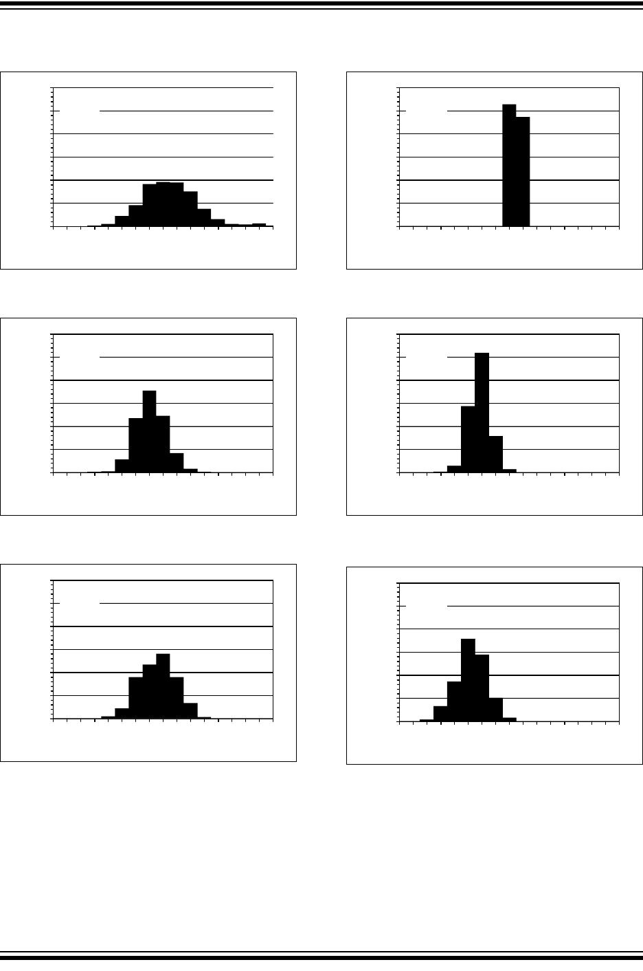
FIGURE 2-7: Temperature Accuracy
Distribution at -15°C.
FIGURE 2-8: Temperature Accuracy
Distribution at 5°C.
FIGURE 2-9: Temperature Accuracy
Distribution at 65°C.
FIGURE 2-10: Temperature Accuracy
Distribution at 105°C.
FIGURE 2-11: Temperature Accuracy
Distribution at 115°C.
FIGURE 2-12: Temperature Accuracy
Distribution at 125°C.
0%
10%
20%
30%
40%
50%
60%
-
4
.
0
-
2
.
0
0
.
0
2
.
0
4
.
0
O
c
c
u
r
r
e
n
c
e
s
Temperature Accuracy (°C)
T
A
= -15\C
V
DD
= 4.1V
492 Units
°
Occurrences
T
A
(°C)
-4.0
-2.0
0.0
2.0
4.0
0%
10%
20%
30%
40%
50%
60%
-
4
.
0
-
2
.
0
0
.
0
2
.
0
4
.
0
O
c
c
u
r
r
e
n
c
e
s
Temperature Accuracy (°C)
T
A
= 5\C
V
DD
= 4.1V
480 Units
Occurrences
°
-4.0
-2.0
0.0
2.0
4.0
T
A
(°C)
0%
10%
20%
30%
40%
50%
60%
-
4
.
0
-
2
.
0
0
.
0
2
.
0
4
.
0
O
c
c
u
r
r
e
n
c
e
s
Temperature Accuracy (°C)
T
A
= 65\C
V
DD
= 4.1V
480 Units
°
T
A
(°C)
-4.0
-2.0
0.0
2.0
4.0
Occurrences
-4.0
-2.0
0.0
2.0
4.0
T
A
(°C)
-4.0
-2.0
0.0
2.0
4.0
T
A
(°C)
°
Occurrences
0%
10%
20%
30%
40%
50%
60%
-
4
.
0
-
2
.
0
0
.
0
2
.
0
4
.
0
O
c
c
u
r
r
e
n
c
e
s
Temperature Accuracy (°C)
T
A
= 105\C
V
DD
= 4.1V
480 Units
°
Occurrences
T
A
(°C)
-4.0
-2.0
0.0
2.0
4.0
0%
10%
20%
30%
40%
50%
60%
-
4
.
0
-
2
.
0
0
.
0
2
.
0
4
.
0
O
c
c
u
r
r
e
n
c
e
s
Temperature Accuracy (°C)
T
A
= 115\C
V
DD
= 4.1V
480 Units
-4.0
-2.0
0.0
2.0
4.0
°
T
A
(°C)
Occurrences
°
0%
10%
20%
30%
40%
50%
60%
-
4
.
0
-
2
.
0
0
.
0
2
.
0
4
.
0
O
c
c
u
r
r
e
n
c
e
s
Temperature Accuracy (°C)
T
A
= 125\C
V
DD
= 4.1V
480 Units
Occurrences
T
A
(°C)
-4.0
-2.0
0.0
2.0
4.0
°
MCP9501/2/3/4
DS22268A-page 6 © 2011 Microchip Technology Inc.
3.0 PIN DESCRIPTIONS
TABLE 3-1: PIN FUNCTION TABLE
3.1 Ground (GND)
The GND pin is the system ground pin. Pin 2 must be
connected to system ground. Pin 1 can also be
connected to system ground which would provide
better thermal conduction to the die.
3.2 Hysteresis Input (HYS)
This is an input pin which can be connected to V
DD
or
GND to select output hysteresis. Either 2°C
(HYST = GND) or 10°C (HYST = V
DD
)
of typical
hysteresis can be selected.
3.3 Power Pin (V
DD
)
The operating voltage range, as specified in the DC
electrical specification table, is applied on this pin.
3.4 Switch Output (Output)
This output is triggered when temperature rises or falls
beyond the programmed trip temperature threshold.
MCP9501/3 require an external pull-up resistor.
MCP9501/2/3/4
Symbol Description
SOT-23-5
1 GND Ground
2 GND Ground (must be connected to ground)
3 HYST Hysteresis Selection Input:
HYST = GND Hysteresis is 2°C (typical)
HYST = V
DD
Hysteresis is 10°C (typical)
4V
DD
Power pin
5 Output Output Options:
MCP9501 Open-Drain, Active-Low Output (Hot-Option)
MCP9502 Push-Pull, Active-High Output (Hot-Option)
MCP9503 Open-Drain, Active-Low Output (Cold-Option)
MCP9504 Push-Pull, Active-High Output (Cold-Option)

MCP9502PT-065E/OT

Mfr. #:
Manufacturer:
Description:
Board Mount Temperature Sensors Factory Prog Temp SW Act Hi puch-pull out
Lifecycle:
New from this manufacturer.
Delivery:
DHL FedEx Ups TNT EMS
Payment:
T/T Paypal Visa MoneyGram Western Union