MC10EP445, MC100EP445
http://onsemi.com
4
Table 3. ATTRIBUTES
Characteristics Value
Internal Input Pulldown Resistor
75 k
Internal Input Pull−up Resistor N/A
ESD Protection Human Body Model
Machine Model
Charged Device Model
> 2 kV
> 200 V
> 2 kV
Moisture Sensitivity, Indefinite Time Out of Drypack (Note 1) Pb Pkg Pb−Free Pkg
LQFP−32
QFN−32
Level 2
N/A
Level 2
Level 1
Flammability Rating Oxygen Index: 28 to 34 UL 94 V−0 @ 0.125 in
Transistor Count 993 Devices
Meets or exceeds JEDEC Spec EIA/JESD78 IC Latchup Test
1. For additional information, see Application Note AND8003/D.
Table 4. MAXIMUM RATINGS
Symbol Parameter Condition 1 Condition 2 Rating Unit
V
CC
PECL Mode Power Supply V
EE
= 0 V 6 V
V
EE
NECL Mode Power Supply V
CC
= 0 V −6 V
V
I
PECL Mode Input Voltage
NECL Mode Input Voltage
V
EE
= 0 V
V
CC
= 0 V
V
I
V
CC
V
I
V
EE
6
−6
V
V
I
out
Output Current Continuous
Surge
50
100
mA
mA
I
BB
V
BB
Sink/Source ± 0.5 mA
T
A
Operating Temperature Range −40 to +85 °C
T
stg
Storage Temperature Range −65 to +150 °C
JA
Thermal Resistance (Junction−to−Ambient) 0 lfpm
500 lfpm
32 LQFP
32 LQFP
80
55
°C/W
°C/W
JC
Thermal Resistance (Junction−to−Case) Standard Board 32 LQFP 12 to 17 °C/W
JA
Thermal Resistance (Junction−to−Ambient) 0 lfpm
500 lfpm
QFN−32
QFN−32
31
27
°C/W
°C/W
JC
Thermal Resistance (Junction−to−Case) 2S2P QFN−32 12 °C/W
T
sol
Wave Solder Pb−Free <2 to 3 sec @ 260°C 265 °C
Stresses exceeding those listed in the Maximum Ratings table may damage the device. If any of these limits are exceeded, device functionality
should not be assumed, damage may occur and reliability may be affected.
MC10EP445, MC100EP445
http://onsemi.com
5
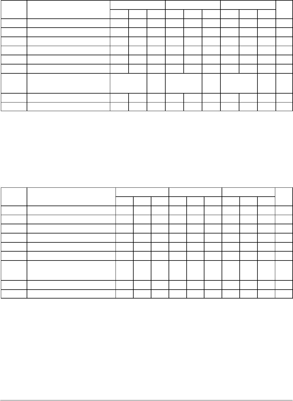
Table 5. 10EP DC CHARACTERISTICS, PECL V
CC
= 3.3 V, V
EE
= 0 V (Note 2)
Symbol
Characteristic
−40°C 25°C 85°C
Unit
Min Typ Max Min Typ Max Min Typ Max
I
EE
Power Supply Current 95 119 143 98 122 146 100 125 150 mA
V
OH
Output HIGH Voltage (Note 3) 2165 2290 2415 2230 2355 2480 2290 2415 2540 mV
V
OL
Output LOW Voltage (Note 3) 1365 1490 1615 1430 1555 1680 1490 1615 1740 mV
V
IH
Input HIGH Voltage (Single−Ended) 2090 2415 2155 2480 2215 2540 mV
V
IL
Input LOW Voltage (Single−Ended) 1365 1690 1460 1755 1490 1815 mV
V
BB
Output Voltage Reference 1790 1890 1990 1855 1955 2055 1915 2015 2115 mV
V
IHCMR
Input HIGH Voltage Common Mode
Range (Differential Configuration)
(Note 4)
2.0 3.3 2.0 3.3 2.0 3.3 V
I
IH
Input HIGH Current 150 150 150
A
I
IL
Input LOW Current 0.5 0.5 0.5
A
NOTE: Device will meet the specifications after thermal equilibrium has been established when mounted in a test socket or printed circuit
board with maintained transverse airflow greater than 500 lfpm. Electrical parameters are guaranteed only over the declared
operating temperature range. Functional operation of the device exceeding these conditions is not implied. Device specification limit
values are applied individually under normal operating conditions and not valid simultaneously.
2. Input and output parameters vary 1:1 with V
CC
. V
EE
can vary +0.3 V to −2.2 V.
3. All loading with 50 to V
CC
− 2.0 V.
4. V
IHCMR
min varies 1:1 with V
EE
, V
IHCMR
max varies 1:1 with V
CC
. The V
IHCMR
range is referenced to the most positive side of the differential
input signal.
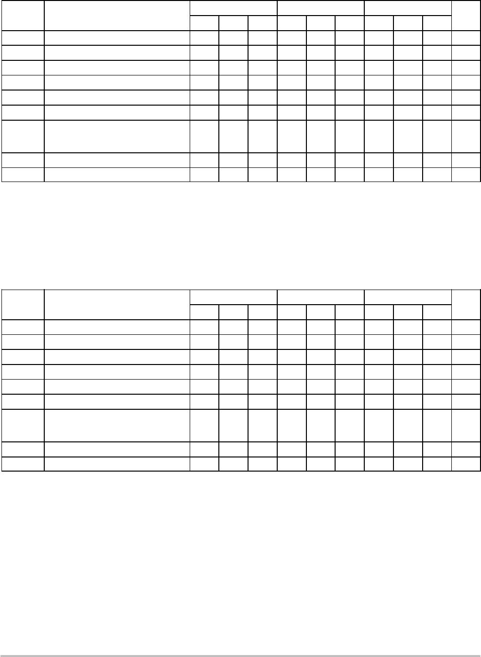
Table 6. 10EP DC CHARACTERISTICS, PECL V
CC
= 5.0 V, V
EE
= 0 V (Note 5)
Symbol
Characteristic
−40°C 25°C 85°C
Unit
Min Typ Max Min Typ Max Min Typ Max
I
EE
Power Supply Current (Note 6) 95 119 143 98 122 146 100 125 150 mA
V
OH
Output HIGH Voltage (Note 7) 3865 3990 4115 3930 4055 4180 3990 4115 4240 mV
V
OL
Output LOW Voltage (Note 7) 3065 3190 3315 3130 3255 3380 3190 3315 3440 mV
V
IH
Input HIGH Voltage (Single−Ended) 3790 4115 3855 4180 3915 4240 mV
V
IL
Input LOW Voltage (Single−Ended) 3065 3390 3130 3455 3190 3515 mV
V
BB
Output Voltage Reference 3490 3590 3690 3555 3655 3755 3615 3715 3815 mV
V
IHCMR
Input HIGH Voltage Common Mode
Range (Differential Configuration)
(Note 8)
2.0 5.0 2.0 5.0 2.0 5.0 V
I
IH
Input HIGH Current 150 150 150
A
I
IL
Input LOW Current 0.5 0.5 0.5
A
NOTE: Device will meet the specifications after thermal equilibrium has been established when mounted in a test socket or printed circuit
board with maintained transverse airflow greater than 500 lfpm. Electrical parameters are guaranteed only over the declared
operating temperature range. Functional operation of the device exceeding these conditions is not implied. Device specification limit
values are applied individually under normal operating conditions and not valid simultaneously.
5. Input and output parameters vary 1:1 with V
CC
. V
EE
can vary +2.0 V to −0.5 V.
6. Required 500 lfpm air flow when using +5 V power supply. For (V
CC
− V
EE
) >3.3 V, 5 to 10 in line with V
EE
required for maximum thermal
protection at elevated temperatures. Recommend V
CC
−V
EE
operation at 3.3 V.
7. All loading with 50 to V
CC
− 2.0 V.
8. V
IHCMR
min varies 1:1 with V
EE
, V
IHCMR
max varies 1:1 with V
CC
. The V
IHCMR
range is referenced to the most positive side of the differential
input signal.
MC10EP445, MC100EP445
http://onsemi.com
6
Table 7. 10EP DC CHARACTERISTICS, NECL V
CC
= 0 V, V
EE
= −5.5 V to −3.0 V (Note 9)
Symbol
Characteristic
−40°C 25°C 85°C
Unit
Min Typ Max Min Typ Max Min Typ Max
I
EE
Power Supply Current (Note 10) 95 119 143 98 122 146 100 125 150 mA
V
OH
Output HIGH Voltage (Note 11) −1135 −1010 −885 −1070 −945 −820 −1010 −885 −760 mV
V
OL
Output LOW Voltage (Note 11) −1935 −1810 −1685 −1870 −1745 −1620 −1810 −1685 −1560 mV
V
IH
Input HIGH Voltage (Single−Ended) −1210 −885 1145 −820 −1085 −760 mV
V
IL
Input LOW Voltage (Single−Ended) −1935 −1610 −1870 −1545 −1810 −1485 mV
V
BB
Output Voltage Reference −1510 −1410 −1310 −1445 −1345 −1245 −1385 −1285 −1185 mV
V
IHCMR
Input HIGH Voltage Common Mode
Range (Differential Configuration)
(Note 12)
V
EE
+2.0 0.0 V
EE
+2.0 0.0 V
EE
+2.0 0.0 V
I
IH
Input HIGH Current 150 150 150
A
I
IL
Input LOW Current 0.5 0.5 0.5
A
NOTE: Device will meet the specifications after thermal equilibrium has been established when mounted in a test socket or printed circuit
board with maintained transverse airflow greater than 500 lfpm. Electrical parameters are guaranteed only over the declared
operating temperature range. Functional operation of the device exceeding these conditions is not implied. Device specification limit
values are applied individually under normal operating conditions and not valid simultaneously.
9. Input and output parameters vary 1:1 with V
CC
.
10.Required 500 lfpm air flow when using −5 V power supply. For (V
CC
− V
EE
) >3.3 V, 5 to 10 in line with V
EE
required for maximum thermal
protection at elevated temperatures. Recommend V
CC
−V
EE
operation at 3.3 V.
11. All loading with 50 to V
CC
− 2.0 V.
12.V
IHCMR
min varies 1:1 with V
EE
, V
IHCMR
max varies 1:1 with V
CC
. The V
IHCMR
range is referenced to the most positive side of the differential
input signal.
Table 8. 100EP DC CHARACTERISTICS, PECL V
CC
= 3.3 V, V
EE
= 0 V (Note 13)
Symbol
Characteristic
−40°C 25°C 85°C
Unit
Min Typ Max Min Typ Max Min Typ Max
I
EE
Power Supply Current 95 119 143 98 122 146 100 125 150 mA
V
OH
Output HIGH Voltage (Note 14) 2155 2280 2405 2155 2280 2405 2155 2280 2405 mV
V
OL
Output LOW Voltage (Note 14) 1305 1480 1605 1305 1480 1605 1305 1480 1605 mV
V
IH
Input HIGH Voltage (Single−Ended) 2075 2420 2075 2420 2075 2420 mV
V
IL
Input LOW Voltage (Single−Ended) 1305 1675 1305 1675 1305 1675 mV
V
BB
Output Voltage Reference 1775 1875 1975 1775 1875 1975 1775 1875 1975 mV
V
IHCMR
Input HIGH Voltage Common Mode
Range (Differential Configuration)
(Note 15)
2.0 3.3 2.0 3.3 2.0 3.3 V
I
IH
Input HIGH Current 150 150 150
A
I
IL
Input LOW Current 0.5 0.5 0.5
A
NOTE: Device will meet the specifications after thermal equilibrium has been established when mounted in a test socket or printed circuit
board with maintained transverse airflow greater than 500 lfpm. Electrical parameters are guaranteed only over the declared
operating temperature range. Functional operation of the device exceeding these conditions is not implied. Device specification limit
values are applied individually under normal operating conditions and not valid simultaneously.
13.Input and output parameters vary 1:1 with V
CC
. V
EE
can vary +0.3 V to −2.2 V.
14.All loading with 50 to V
CC
− 2.0 V.
15.V
IHCMR
min varies 1:1 with V
EE
, V
IHCMR
max varies 1:1 with V
CC
. The V
IHCMR
range is referenced to the most positive side of the differential
input signal.

MC100EP445FAG

Mfr. #:
Manufacturer:
ON Semiconductor
Description:
Serial to Parallel Logic Converters 3.3V/5V ECL 8-Bit Serial to Parallel
Lifecycle:
New from this manufacturer.
Delivery:
DHL FedEx Ups TNT EMS
Payment:
T/T Paypal Visa MoneyGram Western Union