MC10EP445, MC100EP445
http://onsemi.com
7
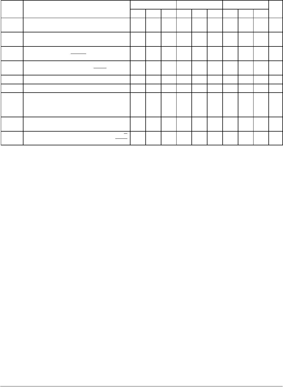
Table 9. 100EP DC CHARACTERISTICS, PECL V
CC
= 5.0 V, V
EE
= 0 V (Note 16)
Symbol
Characteristic
−40°C 25°C 85°C
Unit
Min Typ Max Min Typ Max Min Typ Max
I
EE
Power Supply Current (Note 17) 95 119 143 98 122 146 100 125 150 mA
V
OH
Output HIGH Voltage (Note 18) 3855 3980 4105 3855 3980 4105 3855 3980 4105 mV
V
OL
Output LOW Voltage (Note 18) 3005 3180 3305 3005 3180 3305 3005 3180 3305 mV
V
IH
Input HIGH Voltage (Single−Ended) 3775 4120 3775 4120 3775 4120 mV
V
IL
Input LOW Voltage (Single−Ended) 3005 3375 3005 3375 3005 3375 mV
V
BB
Output Voltage Reference 3475 3575 3675 3475 3575 3675 3475 3575 3675 mV
V
IHCMR
Input HIGH Voltage Common Mode
Range (Differential Configuration)
(Note 19)
2.0 5.0 2.0 5.0 2.0 5.0 V
I
IH
Input HIGH Current 150 150 150
A
I
IL
Input LOW Current 0.5 0.5 0.5
A
NOTE: Device will meet the specifications after thermal equilibrium has been established when mounted in a test socket or printed circuit
board with maintained transverse airflow greater than 500 lfpm. Electrical parameters are guaranteed only over the declared
operating temperature range. Functional operation of the device exceeding these conditions is not implied. Device specification limit
values are applied individually under normal operating conditions and not valid simultaneously.
16.Input and output parameters vary 1:1 with V
CC
. V
EE
can vary +2.0 V to −0.5 V.
17.Required 500 lfpm air flow when using +5 V power supply. For (V
CC
− V
EE
) >3.3 V, 5 to 10 in line with V
EE
required for maximum thermal
protection at elevated temperatures. Recommend V
CC
−V
EE
operation at 3.3 V.
18.All loading with 50 to V
CC
− 2.0 V.
19.V
IHCMR
min varies 1:1 with V
EE
, V
IHCMR
max varies 1:1 with V
CC
. The V
IHCMR
range is referenced to the most positive side of the differential
input signal.
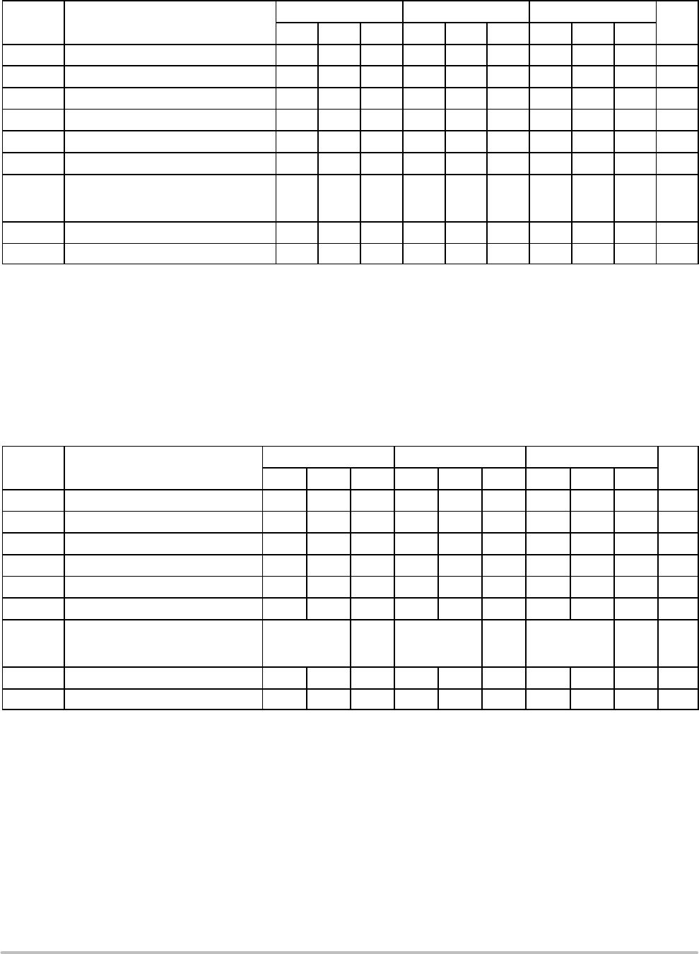
Table 10. 100EP DC CHARACTERISTICS, NECL V
CC
= 0 V, V
EE
= −5.5 V to −3.0 V (Note 20)
Symbol
Characteristic
−40°C 25°C 85°C
Unit
Min Typ Max Min Typ Max Min Typ Max
I
EE
Power Supply Current (Note 21) 95 119 143 98 122 146 100 125 150 mA
V
OH
Output HIGH Voltage (Note 22) −1145 −1020 −895 −1145 −1020 −895 −1145 −1020 −895 mV
V
OL
Output LOW Voltage (Note 22) −1995 −1820 −1695 −1995 −1820 −1695 −1995 −1820 −1695 mV
V
IH
Input HIGH Voltage (Single−Ended) −1225 −880 −1225 −880 −1225 −880 mV
V
IL
Input LOW Voltage (Single−Ended) −1995 −1625 −1995 −1625 −1995 −1625 mV
V
BB
Output Voltage Reference −1525 −1425 −1325 −1525 −1425 −1325 −1525 −1425 −1325 mV
V
IHCMR
Input HIGH Voltage Common Mode
Range (Differential Configuration)
(Note 23)
V
EE
+ 2.0 0.0 V
EE
+ 2.0 0.0 V
EE
+ 2.0 0.0 V
I
IH
Input HIGH Current 150 150 150
A
I
IL
Input LOW Current 0.5 0.5 0.5
A
NOTE: Device will meet the specifications after thermal equilibrium has been established when mounted in a test socket or printed circuit
board with maintained transverse airflow greater than 500 lfpm. Electrical parameters are guaranteed only over the declared
operating temperature range. Functional operation of the device exceeding these conditions is not implied. Device specification limit
values are applied individually under normal operating conditions and not valid simultaneously.
20.Input and output parameters vary 1:1 with V
CC
.
21.Required 500 lfpm air flow when using −5.0 V power supply. For (V
CC
− V
EE
) > 3.3 V, 5 to 10 in line with V
EE
required for maximum
thermal protection at elevated temperatures. Recommend V
CC
− V
EE
operation at v 3.3 V.
22.All loading with 50 to V
CC
− 2.0 V.
23.V
IHCMR
min varies 1:1 with V
EE
, V
IHCMR
max varies 1:1 with V
CC
. The V
IHCMR
range is referenced to the most positive side of the differential
input signal.