Hand-Held Portable
Applications
Medical Instruments
Battery-Powered Test
Equipment
Solar-Powered Remote
Systems
Received-Signal-Strength
Indicators
System Supervision
General Description
The MAX1136–MAX1139 low-power, 10-bit, multichannel
analog-to-digital converters (ADCs) feature internal
track/hold (T/H), voltage reference, clock, and an
I
2
C-compatible 2-wire serial interface. These devices
operate from a single supply of 2.7V to 3.6V (MAX1137/
MAX1139) or 4.5V to 5.5V (MAX1136/MAX1138) and
require only 670µA at the maximum sampling rate of
94.4ksps. Supply current falls below 230µA for sampling
rates under 46ksps. AutoShutdown™ powers down the
devices between conversions, reducing supply current to
less than 1µA at low throughput rates. The
MAX1136/MAX1137 have four analog input channels
each, while the MAX1138/MAX1139 have 12 analog input
channels each. The fully differential analog inputs are
software configurable for unipolar or bipolar, and single
ended or differential operation.
The full-scale analog input range is determined by the
internal reference or by an externally applied reference
voltage ranging from 1V to V
DD
. The MAX1137/
MAX1139 feature a 2.048V internal reference and the
MAX1136/MAX1138 feature a 4.096V internal reference.
The MAX1136/MAX1137 are available in an 8-pin µMAX
®
package. The MAX1138/MAX1139 are available in a
16-pin QSOP package. The MAX1136–MAX1139 are
guaranteed over the extended temperature range
(-40°C to +85°C). For pin-compatible 12-bit parts, refer to
the MAX1236–MAX1239 data sheet. For pin-compatible
8-bit parts, refer to the MAX1036–MAX1039 data sheet.
Applications
Features
o High-Speed I
2
C-Compatible Serial Interface
400kHz Fast Mode
1.7MHz High-Speed Mode
o Single-Supply
2.7V to 3.6V (MAX1137/MAX1139)
4.5V to 5.5V (MAX1136/MAX1138)
o Internal Reference
2.048V (MAX1137/MAX1139)
4.096V (MAX1136/MAX1138)
o External Reference: 1V to V
DD
o Internal Clock
o 4-Channel Single-Ended or 2-Channel Fully
Differential (MAX1136/MAX1137)
o 12-Channel Single-Ended or 6-Channel Fully
Differential (MAX1138/MAX1139)
o Internal FIFO with Channel-Scan Mode
o Low Power
670µA at 94.4ksps
230µA at 40ksps
60µA at 10ksps
6µA at 1ksps
0.5µA in Power-Down Mode
o Software-Configurable Unipolar/Bipolar
o Small Packages
8-Pin µMAX (MAX1136/MAX1137)
16-Pin QSOP (MAX1138/MAX1139)
MAX1136–MAX1139
2.7V to 3.6V and 4.5V to 5.5V, Low-Power,
4-/12-Channel, 2-Wire Serial 10-Bit ADCs
________________________________________________________________
Maxim Integrated Products
1
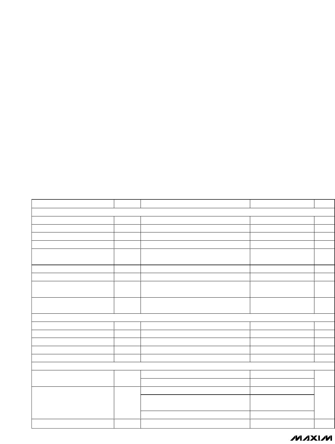
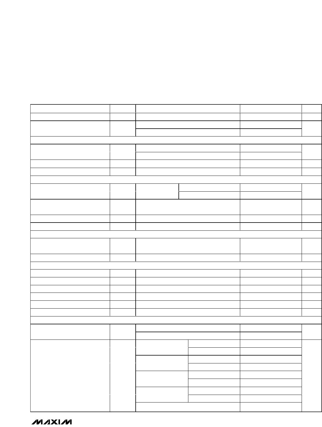
Ordering Information
19-2334; Rev 6; 3/10
For pricing, delivery, and ordering information, please contact Maxim Direct at 1-888-629-4642,
or visit Maxim’s website at www.maxim-ic.com.
Pin Configurations and Typical Operating Circuit appear at
end of data sheet.
PART TEMP RANGE
PIN-
PACKAGE
I
2
C SLAVE
ADDRESS
MAX1136EUA+ -40°C to +85°C 8 µMAX 0110100
MAX1137EUA+ -40°C to +85°C 8 µMAX 0110100
MAX1138EEE+ -40°C to +85°C 16 QSOP 0110101
MAX1139EEE+ -40°C to +85°C 16 QSOP 0110101
Selector Guide
PART
INPUT
CHANNELS
INTERNAL
REFERENCE
(V)
SUPPLY
VOLTAGE
(V)
INL
(LSB)
MAX1136 4 4.096 4.5 to 5.5 ±1
MAX1137 4 2.048 2.7 to 3.6 ±1
MAX1138 12 4.096 4.5 to 5.5 ±1
MAX1139 12 2.048 2.7 to 3.6 ±1
AutoShutdown is a trademark of Maxim Integrated Products, Inc.
µMAX is a registered trademark of Maxim Integrated Products, Inc.
+
Denotes a lead(Pb)-free/RoHS-compliant package.
MAX1136–MAX1139
2.7V to 3.6V and 4.5V to 5.5V, Low-Power,
4-/12-Channel, 2-Wire Serial 10-Bit ADCs
2 _______________________________________________________________________________________
ABSOLUTE MAXIMUM RATINGS
ELECTRICAL CHARACTERISTICS
(V
DD
= 2.7V to 3.6V (MAX1137/MAX1139), V
DD
= 4.5V to 5.5V (MAX1136/MAX1138), V
REF
= 2.048V (MAX1137/MAX1139), V
REF
=
4.096V (MAX1136/MAX1138), f
SCL
= 1.7MHz, T
A
= T
MIN
to T
MAX
, unless otherwise noted. Typical values are at T
A
= +25°C. See
Tables 1–5 for programming notation.)
Stresses beyond those listed under “Absolute Maximum Ratings” may cause permanent damage to the device. These are stress ratings only, and functional
operation of the device at these or any other conditions beyond those indicated in the operational sections of the specifications is not implied. Exposure to
absolute maximum rating conditions for extended periods may affect device reliability.
V
DD
to GND..............................................................-0.3V to +6V
AIN0–AIN11,
REF to GND............-0.3V to the lower of (V
DD
+ 0.3V) and 6V
SDA, SCL to GND.....................................................-0.3V to +6V
Maximum Current Into Any Pin .........................................±50mA
Continuous Power Dissipation (T
A
= +70°C)
8-Pin µMAX (derate 5.9mW/°C above +70°C) ..........470.6mW
16-Pin QSOP (derate 8.3mW/°C above +70°C)........666.7mW
Operating Temperature Range ...........................-40°C to +85°C
Junction Temperature......................................................+150°C
Storage Temperature Range .............................-60°C to +150°C
Lead Temperature (soldering, 10s) .................................+300°C
Soldering Temperature (reflow) .......................................+260°C
PARAMETER SYMBOL CONDITIONS MIN TYP MAX UNITS
DC ACCURACY (Note 1)
Resolution 10 Bits
Relative Accuracy INL (Note 2) ±1 LSB
Differential Nonlinearity DNL No missing codes over temperature ±1 LSB
Offset Error ±1 LSB
Offset-Error Temperature
Coefficient
Relative to FSR 0.3 ppm/°C
Gain Error (Note 3) ±1 LSB
Gain-Temperature Coefficient Relative to FSR 0.3 ppm/°C
Channel-to-Channel Offset
Matching
±0.1 LSB
Channel-to-Channel Gain
Matching
±0.1 LSB
DYNAMIC PERFORMANCE (f
IN(SINE-WAVE)
= 10kHz, V
IN(P-P)
= V
REF
, f
SAMPLE
= 94.4ksps)
Signal-to-Noise Plus Distortion SINAD 60 dB
Total Harmonic Distortion THD Up to the 5th harmonic -70 dB
Spurious Free Dynamic Range SFDR 70 dB
Full-Power Bandwidth SINAD > 57dB 3.0 MHz
Full-Linear Bandwidth -3dB point 5.0 MHz
CONVERSION RATE
Internal clock 6.8
Conversion Time (Note 4) t
CONV
External clock 10.6
µs
Internal clock, SCAN[1:0] = 01 53
Internal clock, SCAN[1:0] = 00
CS[3:0] = 1011 (MAX1138/MAX1139)
53
Throughput Rate f
SAMPLE
External clock 94.4
ksps
Track/Hold Acquisition Time 800 ns
MAX1136–MAX1139
2.7V to 3.6V and 4.5V to 5.5V, Low-Power,
4-/12-Channel, 2-Wire Serial 10-Bit ADCs
_______________________________________________________________________________________ 3
ELECTRICAL CHARACTERISTICS (continued)
(V
DD
= 2.7V to 3.6V (MAX1137/MAX1139), V
DD
= 4.5V to 5.5V (MAX1136/MAX1138), V
REF
= 2.048V (MAX1137/MAX1139), V
REF
=
4.096V (MAX1136/MAX1138), f
SCL
= 1.7MHz, T
A
= T
MIN
to T
MAX
, unless otherwise noted. Typical values are at T
A
= +25°C. See
Tables 1–5 for programming notation.)
PARAMETER SYMBOL CONDITIONS MIN TYP MAX UNITS
Internal Clock Frequency 2.8 MHz
External clock, fast mode 60
Aperture Delay (Note 5) t
AD
External clock, high-speed mode 30
ns
ANALOG INPUT (AIN0–AIN11)
Unipolar 0 V
REF
Input-Voltage Range, Single-
Ended and Differential (Note 6)
Bipolar 0 ±V
REF
/2
V
Input Multiplexer Leakage Current ON/OFF leakage current, VAIN_ = 0 or VDD ±0.01 ±1 µA
Input Capacitance CIN 22 pF
INTERNAL REFERENCE (Note 7)
MAX1137/MAX1139 1.968 2.048 2.128
Reference Voltage VREF T
A
= +25°C
MAX1136/MAX1138 3.939 4.096 4.256
V
Reference-Voltage Temperature
Coefficient
TCVREF 25 ppm/°C
REF Short-Circuit Current 2mA
REF Source Impedance 1.5 k
EXTERNAL REFERENCE
REF Input-Voltage Range VREF (Note 8) 1 VDD V
REF Input Current IREF f
SAMPLE
= 94.4ksps 40 µA
DIGITAL INPUTS/OUTPUTS (SCL, SDA)
Input High Voltage V
IH
0.7
V
DD
V
Input Low Voltage V
IL
0.3
V
DD
V
Input Hysteresis V
HYST
0.1
V
DD
V
Input Current I
IN
V
IN
0 to V
DD
±10 µA
Input Capacitance C
IN
15 pF
Output Low Voltage V
OL
I
SINK
= 3mA 0.4 V
POWER REQUIREMENTS
MAX1137/MAX1139 2.7 3.6
Supply Voltage V
DD
MAX1136/MAX1138 4.5 5.5
V
Internal reference 900 1150
f
SAMPLE
= 94.4ksps
external clock
External reference 670 900
Internal reference 530
f
SAMPLE
= 40ksps
internal clock
External reference 230
Internal reference 380
f
SAMPLE
= 10ksps
internal clock
External reference 60
Internal reference 330
f
SAMPLE
=1ksps
internal clock
External reference 6
Supply Current I
DD
Shutdown (internal reference OFF) 0.5 10
µA

MAX1138EEE+T

Mfr. #:
Manufacturer:
Maxim Integrated
Description:
Analog to Digital Converters - ADC 10-Bit 12Ch 94.4ksps 5.5V Precision ADC
Lifecycle:
New from this manufacturer.
Delivery:
DHL FedEx Ups TNT EMS
Payment:
T/T Paypal Visa MoneyGram Western Union