LTC2920-1/LTC2920-2
14
292012fa
APPLICATIO S I FOR ATIO
WUU
U
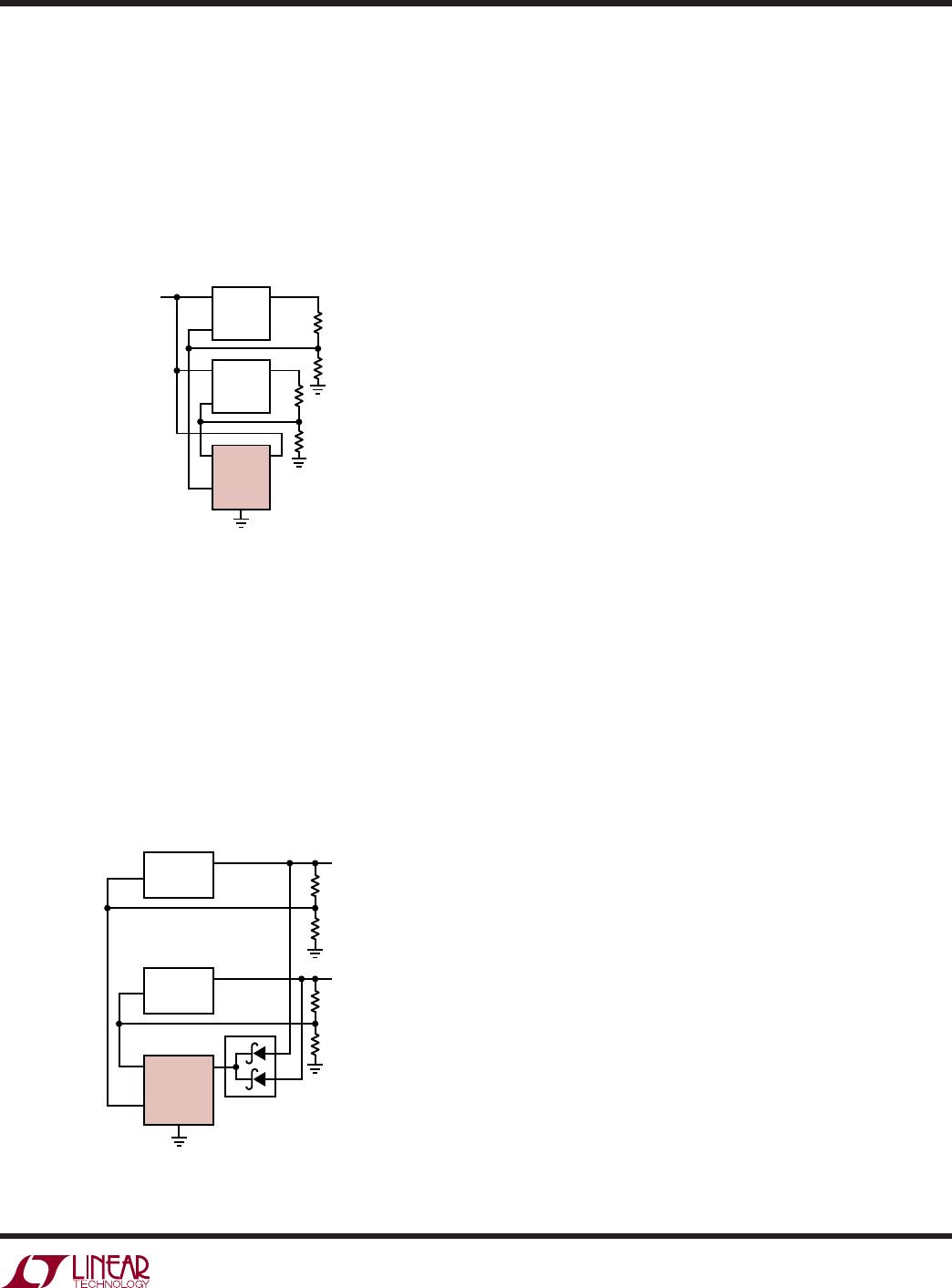
Figure 19. V
CC
Power Filtering
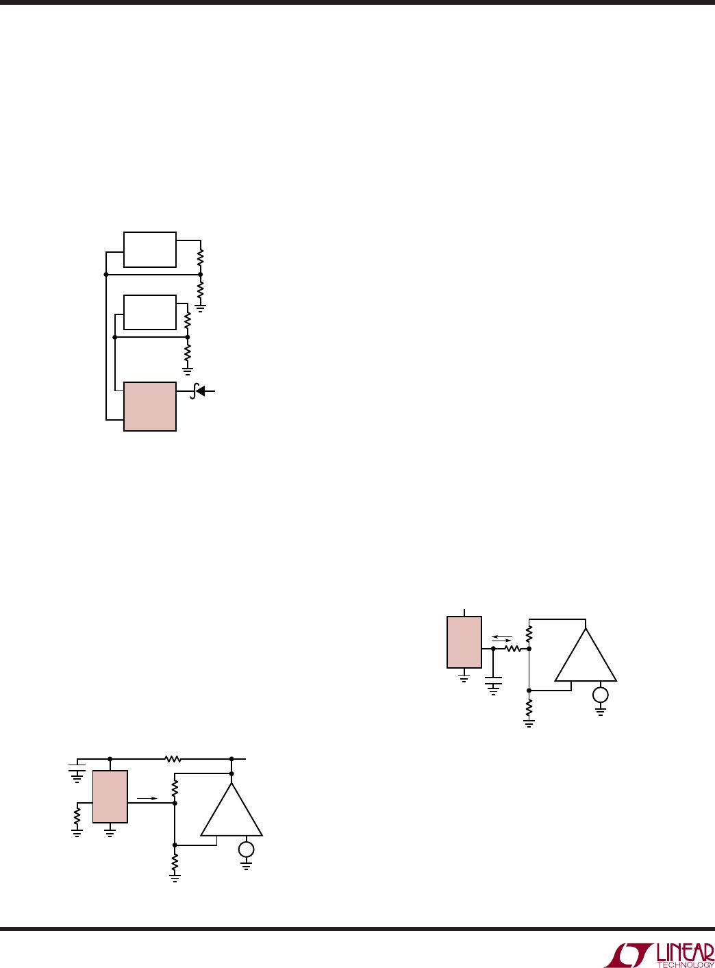
Figure 20. Slowing Down V
MARGIN
R
SET
2920-1/2 F19
R
G
C
BYP
0.1μF
V
PSOUT
= 3.3V
I
MARGIN
=
100μA
I
M
R
S
V
CC
GND
LTC2920
+
–
R
F
V
REF
= 1.2V
+
–
R
BYP
360Ω
2920-1/2 F20
1.5k
C
S
0.2μF
I
MARGIN
I
M
R
S
5k
V
CC
3.3V
GND
LTC2920
+
–
5k
V
REF
1.21V
+
–
voltage. The value of the R
BYP
resistor can then be calcu-
lated by:
R
BYP
= V
RB
/I
CCMAX
= 0.5V/1.4mA = 360Ω
With C
BYP
= 0.1μF, this will provide a pole at 2870Hz. If
additional filtering is necessary, the value of C
BYP
can be
increased. In this example, if C
BYP
is increased from 0.1μF
to 1μF, the pole would now be at 287Hz.
to Figure 20, Slowing Down V
MARGIN
, a capacitor (C
S
) and
a resistor (R
S
) have been added to the power supply model
described in previous applications sections. To choose
R
S
, the voltage at the feedback pin of the power supply
must be known. Refer to the power supply manufacturer’s
data sheet for this voltage. The voltage at the I
M
pin must
be within specified limits of the LTC2920, including the
voltage drop across R
S
. In the example below, the power
supply feedback pin voltage is 1.21V, I
MARGIN
is 100μA
and V
CC
is 3.3V. To maintain LTC2920 current accuracy,
the voltage at the I
M
pin must be between 0.58V and
(V
CC
– 1) or 2.3V (in the low current range). A reasonable
value for the voltage drop across R
S
is 0.5V. The value of
R
S
is then:
R
S
= V
RS
/I
MARGIN
= 0.5V/100μA = 5k
Assuming the desired RC time constant is 1ms, C
S
is
calculated by:
C
S
= T
RC
/R
S
= 1ms/5k = 0.2μF
Note: When C
S
and R
S
are used, an additional pole and a
zero are added to the power supply feedback loop. It is
beyond the scope of this data sheet to predict the behavior
of all power supplies but, in general, as long as the smaller
of the two feedback resistors is no larger than 2 • R
S
, the
effect on the power supply stability should be minimal. The
larger R
S
is with respect to the two feedback resistors, the
less effect it will have.
I
M1
LTC2920-2
BAT54C
SCHOTTKY
DIODE
V
POWER
2920-1/2 F18
I
M2
V
CC
POWER SUPPLY 2
FB
POWER SUPPLY 1
FB
OUT
OUT
Figure 18. Diode Connected to V
CC
Controlling I
MARGIN
Turn On and Turn Off Times
Designers of power supply voltage margining circuits
often need to ensure that power supply voltages do not
overshoot or undershoot (the desired margining voltage)
when the margining current is enabled or disabled. The
LTC2920 I
MARGIN
current sourced or sinked at the I
M
pin(s) is reasonably well behaved (see the Typical Perfor-
mance Characteristics curves). The differences in speed
between the various curves is caused by the relative
impedance differences within the LTC2920.
If slower turn on and turn off times are desired, a resistor-
capacitor network can be used at the I
M
pin(s). Referring
Thermal Shutdown
This IC includes overtemperature protection that is in-
tended to protect the device during momentary overload
conditions. Junction temperature will exceed 125°C when
overtemperature protection is active. Continuous opera-
tion above the specified maximum operating junction
temperature may result in device degradation or failure.