LTC2920-1/LTC2920-2
7
292012fa
Knowing the value of the resistors R
F
and R
G
, and the
voltage of V
REF
, V
PSOUT
can be calculated by:
V
PSOUT
= V
REF
• [1+ (R
F
/R
G
)]
Since the op amp keeps its inverting terminal equal to the
noninverting terminal, the voltage at the inverting terminal
between R
F
and R
G
is V
REF
. Knowing the current flowing
in the feedback resistor network, V
PSOUT
can be also
calculated by:
V
PSOUT
= V
REF
+ (I
FB
• R
F
)
This is the voltage on one side of R
F
, plus the voltage
across R
F
. This equation is helpful in understanding how
the LTC2920 changes the power supply output voltage.
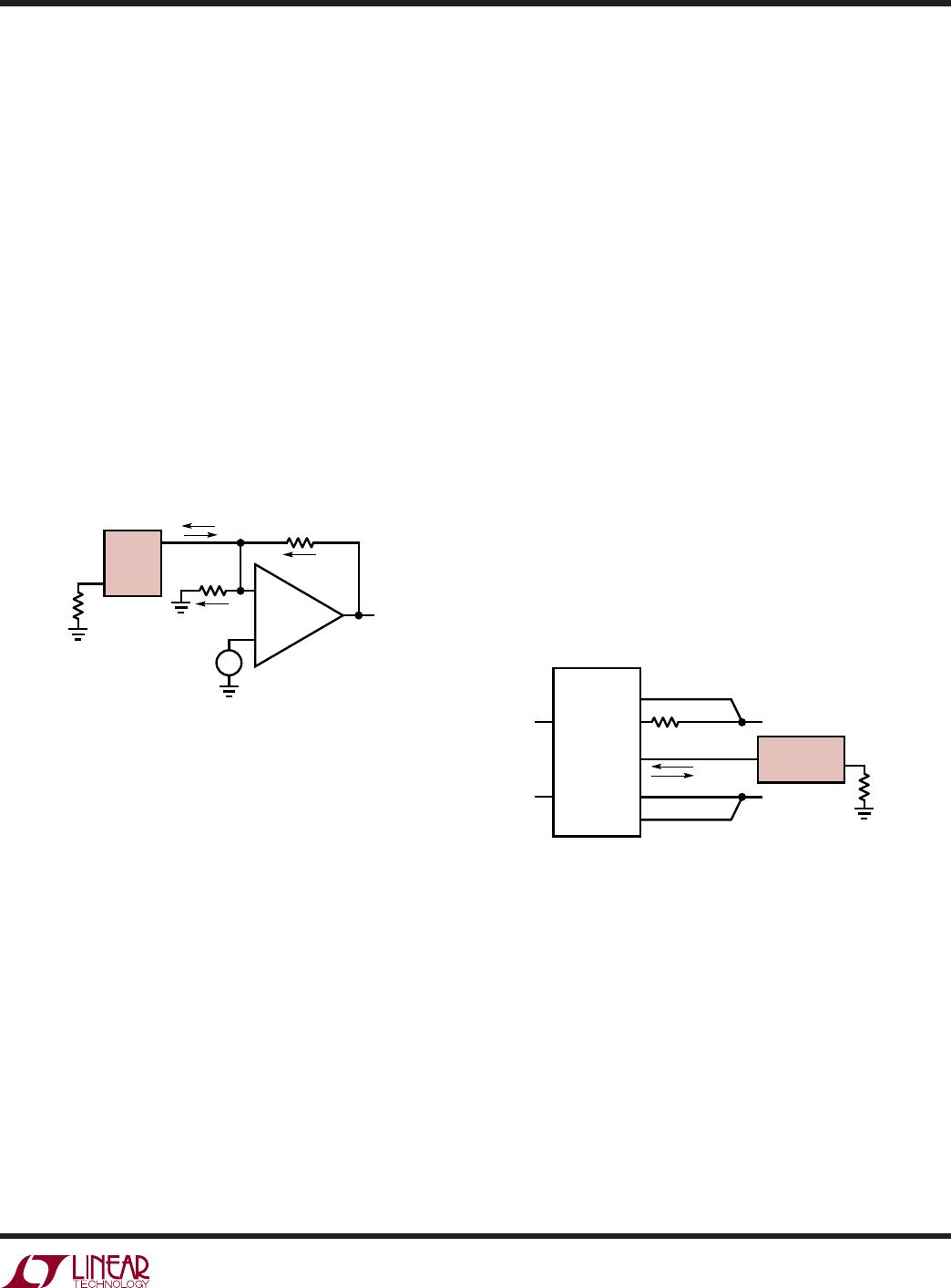
Figure 2 shows the simplified model with the LTC2920
added.
POWER SUPPLY MODULE VOLTAGE MARGINING
Another method of accomplishing voltage margining is
useful for power supply “brick” modules with voltage
adjust pins. Typically, the power supply manufacturer will
design the power supply to be adjusted up or down, using
external resistors connected to the trim pin. The values of
these resistors are usually calculated by the design engi-
neer using two different equations supplied by the manu-
facturer. There is usually one equation for trimming the
voltage up, and another equation for trimming the voltage
down. In most cases, the power supply module is treated
like a “black box” and very little information is given on
how the trimming is accomplished from an internal circuit
standpoint.
Traditionally such power supply modules are margined by
calculating the two resistors, and alternately connecting
each to V
CC
or ground with analog switches or relays.
Figure 3 shows how the LTC2920 can be used in these
applications as well. Using the LTC2920 for these applica-
tions can save a significant amount of PCB real estate
and cost.
APPLICATIO S I FOR ATIO
WUU
U
R
SET
2920-1/2 F02
R
G
V
REF
V
PSOUT
+
R
F
I
MARGIN
I
FB
I
RG
I
M
R
S
LTC2920
+
Figure 2. Simplified Power Supply Model
LTC2920
I
M
R
S
POWER MODULE
SENSE
V
IN
V
O
TRIM
V
IN
+
V
O
+
V
O
V
PSOUT
R
SET
R
SYSTEM
2920-1/2 F03
I
MARGIN
SENSE
+
Figure 3. Margining a Power Supply Module
Power Supply Module Design Considerations
There are usually practical limits to V
O
+
. For instance, V
O
+
usually has upper and lower voltage limits specified by the
power module manufacturer. A common value is 10%
above and 20% below the rated output voltage of the power
supply module. This limit includes V
MARGIN
plus any volt-
age drop across R
SYSTEM
. See the manufacturer’s power
supply module specifications for details. See the “Select-
ing The R
SET
Resistor” section of this datasheet for instruc-
tions on how to choose R
SET
in module applications.
Again in this circuit, the op amp will keep the voltage at its
inverting input at V
REF
. If we add or subtract current at this
node, the delta current will always be added or subtracted
from I
FB
, and never I
RG
. (“±I
MARGIN
” is used rather than a
signed I
MARGIN
value to emphasize the fact that current is
added or subtracted at the feedback pin.) Because of this,
the voltage across R
F
will be:
V
RF
= (I
FBNOM
± I
MARGIN
) • R
F
or
V
RF
= (I
FBNOM
• R
F
) ± (I
MARGIN
• R
F
)
and finally
V
PSOUT
= V
REF
+ (I
FBNOM
• R
F
) ± (I
MARGIN
• R
F
)
Note that the delta voltage V
MARGIN
depends only on
I
MARGIN
and R
F
, not R
G
or V
REF
.
LTC2920-1/LTC2920-2
8
292012fa
Since ΔV
PSOUT
will appear on R
F
as noted in the Overview
section, margin current I
MARGIN
can be calculated by:
I
MARGIN
= ΔV
PSOUT
/R
F
Example: If ΔV
PSOUT
= 0.165V and R
F
= 10k:
I
MARGIN
= 0.165/10k = 16.5μA
If I
MARGIN
is between 5μA and 167μA, use the LTC2920’s
low current range. R
SET
is then calculated by:
R
SET
= 1V/I
MARGIN
= 1V/16.5μA = 60.6k
In this case, R
SET
would be connected between the R
S
pin
and ground.
If I
MARGIN
is between 150μA and 2mA, use the LTC2920’s
high current range. R
SET
is then calculated by:
R
SET
= 1V/(I
MARGIN
/30)
or simply:
R
SET
= 30V/I
MARGIN
APPLICATIO S I FOR ATIO
WUU
U
Example: If the value of the feedback resistor R
F
is 500Ω
in the example above then:
ΔV
PSOUT
= 0.05 • 3.3V = 0.165V
I
MARGIN
= 0.165V/500Ω = 330μA
R
SET
= 30V/I
MARGIN
= 30V/330μA = 90.1k
In this case, R
SET
would be connected between the R
S
pin
and V
CC
.
If I
MARGIN
is less than 5μA, or greater than 2mA, it will be
necessary to adjust both power supply feedback resistors
R
F
and R
G
. Again, this is usually a simple process. It is easy
to calculate the magnitude of the change by dividing the
I
MARGIN
current calculated above by the desired new
SELECTING THE R
SET
RESISTOR
Selecting R
SET
with an Existing Power Supply
Containing a Feedback Pin and Two Feedback
Resistors
Calculating the value of the current setting resistor, R
SET
,
for a power supply with a feedback pin is straight forward.
When the LTC2920 is being added to an existing power
supply design, the power supply feedback resistors R
F
and
R
G
have already been selected. By knowing R
F
, the power
supply output voltage, V
PSOUT
, and the amount to margin,
%change, R
SET
can be calculated.
First, the margining voltage ΔV
PSOUT
can be calculated by
knowing the percentage of the power supply voltage
V
PSOUT
change desired.
ΔV
PSOUT
= %Change • V
PSOUT
Example: If a 3.3V power supply is to be margined by 5%,
then:
ΔV
PSOUT
= 0.05 • 3.3V = 0.165V
Figure 6. 3.3V Supply with 5% Margining (High Range)
R
SET
= 90k
V
CC
2920-1/2 F06
R
G
= 286Ω
V
REF
= 1.2V
V
PSOUT
= 3.3V
+
R
F
= 500Ω
I
MARGIN
= 330μA
I
FB
= 4.2mA
I
M
R
S
LTC2920
+
R
SET
2920-1/2 F04
R
G
V
REF
V
PSOUT
+
R
F
I
MARGIN
I
FB
I
M
R
S
LTC2920
+
Figure 4. Simplified Power Supply Model
R
SET
= 60.6k
2920-1/2 F05
R
G
= 5.76k
V
REF
= 1.2V
V
PSOUT
= 3.3V
+
R
F
= 10k
I
MARGIN
= 16.5μA
I
FB
= 210μA
I
M
R
S
LTC2920
+
Figure 5. 3.3V Supply with 5% Margining (Low Range)
LTC2920-1/LTC2920-2
9
292012fa
I
MARGIN
current. Select a new I
MARGIN
current that is within
one of the two LTC2920’s I
MARGIN
ranges, then calculate
the scaling factor:
I
FACTOR
= I
MARGIN(OLD)
/I
MARGIN(NEW)
The new feedback resistors would then be:
R
F(NEW)
= R
F(OLD)
• I
FACTOR
R
G(NEW)
= R
G(OLD)
• I
FACTOR
And R
SET
can then be calculated as descibed above.
WARNING
In some cases, adjusting the feedback resistors on a
switching supply might require recompensating the power
supply. Please refer to the applications information sup-
plied with the power supply for further information.
APPLICATIO S I FOR ATIO
WUU
U
between the trim pin and the power supply positive voltage
output or the trim pin and the negative power supply
output (ground). The polarity of the voltage trim and trim
resistor configuration are chosen by the manufacturer.
The equations describing the resistor values versus the
desired output voltage changes are typically not linear.
Fortunately, the relationship between trim pin current and
output voltage change is typically linear. The current trim
equation is usually the same (in magnitude) for changing
the output voltage up or down. Once the equation for trim
current is determined, it is much easier to use than trim
resistors. To illustrate this, Figure 8 shows a typical
resistor trim down curve for a power module. Figure 9
shows a typical current trim down curve for the same
power module.
LTC2920
I
M
R
S
POWER MODULE
SENSE
V
IN
V
O
TRIM
V
IN
+
V
O
+
V
O
V
PSOUT
R
SET
2920-1/2 F07
I
MARGIN
SENSE
+
Figure 7. Using a Power Module Trim Pin for Voltage Margining
Selecting the R
SET
Resistor Using Voltage Trim Pins
with ‘Brick’ Type Power Supply Modules
‘Brick’ power supply modules often have a trim pin which
can be used for voltage margining. Figure 7 shows a
typical connection using the LTC2920 for voltage margin-
ing a power supply module.
The amount of current necessary to adjust the output
voltage of the power supply module is not normally given
directly by the manufacturer. However, by using informa-
tion that is supplied by the manufacturer, a measurement
can be made to determine a simple equation that is useful
for power supply module voltage margining.
Typically, the manufacturer will supply two different equa-
tions for selecting trim resistors: one for trimming the
output voltage up and a different one for trimming the
output voltage down. Trim resistors are nominally placed
TRIM VOLTAGE (V)
0 0.1 0.2 0.3 0.4 0.5
TRIM DOWN RESISTANCE (Ω)
2920-1/2 F08
1M
100k
10k
1k
100
10
1
Figure 8. Typical Trim Voltage vs Trim Resistor Curve
TRIM VOLTAGE (V)
0 0.1 0.2 0.3 0.4 0.5
TRIM CURRENT (μA)
2920-1/2 F09
300
250
200
150
100
50
0
Figure 9. Typical Trim Voltage vs Trim Current Curve

LTC2920-1CS5#TRPBF

Mfr. #:
Manufacturer:
Analog Devices Inc.
Description:
Power Management Specialized - PMIC Power Supply Margining Controller
Lifecycle:
New from this manufacturer.
Delivery:
DHL FedEx Ups TNT EMS
Payment:
T/T Paypal Visa MoneyGram Western Union