MAX9692EUB+T

General Description
The MAX9691/MAX9692/MAX9693 are ultra-fast ECL
comparators capable of very short propagation delays.
Their design maintains the excellent DC matching char-
acteristics normally found only in slower comparators.
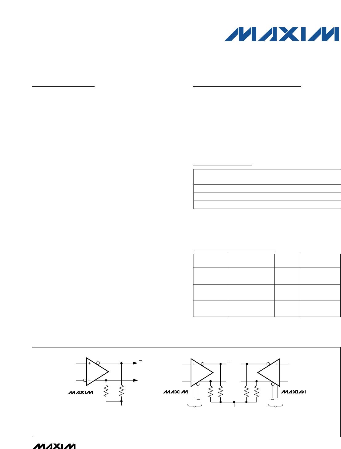
The MAX9691/MAX9692/MAX9693 have differential
inputs and complementary outputs that are fully com-
patible with ECL-logic levels. Output current levels are
capable of driving 50 terminated transmission lines.
The ultra-fast operation makes signal processing possi-
ble at frequencies in excess of 600MHz.
The MAX9692/MAX9693 feature a latch-enable (LE)
function that allows the comparator to be used in a
sample-hold mode. When LE is ECL high, the compara-
tor functions normally. When LE is driven ECL low, the
outputs are forced to an unambiguous ECL-logic state,
dependent on the input conditions at the time of the
latch input transition. If the latch-enable function is not
used on either of the two comparators, the appropriate
LE input must be connected to ground; the companion
LE input must be connected to a high ECL logic level.
These devices are available in SO, QSOP, and tiny
µMAX
®
packages for added space savings.
________________________Applications
High-Speed Line Receivers
Peak Detectors
Threshold Detectors
High-Speed Triggers
Features
o 1.2ns Propagation Delay
o 100ps Propagation Delay Skew
o 150ps Dispersion
o 0.5ns Latch Setup Time
o 0.5ns Latch-Enable Pulse Width
o Available in µMAX and QSOP Packages
o +5V, -5.2V Power Supplies
MAX9691/MAX9692/MAX9693
Single/Dual, Ultra-Fast, ECL-Output
Comparators with Latch Enable
________________________________________________________________
Maxim Integrated Products
1
IN+
R
L
R
L
IN-
V
T
Q OUT
Q OUT
MAX9691
NONINVERTING
INPUT
R
L
R
L
V
T
INVERTING
INPUT
NONINVERTING
INPUT
INVERTING
INPUT
Q OUT
Q OUT
R
L
R
L
LATCH ENABLE
THE OUTPUTS ARE OPEN EMITTERS, REQUIRING EXTERNAL PULLDOWN
RESISTORS. THESE RESISTORS MAY BE IN THE RANGE OF 50TO 200
CONNECTED TO -2.0V, OR 240 TO 2000 CONNECTED TO -5.2V.
MAX9693 MAX9693
LE LE
LATCH ENABLE
LE LE
_________________________________________________________
Functional Diagrams
19-1789; Rev 2; 1/12
Ordering Information
Ordering Information continued at the end of data sheet.
Pin Configurations appear at end of data sheet.
PART
TEMP
RANGE
PIN-PACKAGE
MAX9691EUA -40°C to +85°C 8 µMAX
MAX9691ESA -40°C to +85°C 8 SO
MAX9691EPA -40°C to +85°C 8 PDIP
Selector Guide
PART
COMPARATORS
PER PACKAGE
LATCH
ENABLE
PIN-
PACKAGE
MAX9691 1 No
8 µMAX,
8 SO, 8 PDIP
MAX9692 1 Yes
10 µMAX,
16 SO, 16 PDIP
MAX9693 2 Yes
16 QSOP,
16 SO, 16 PDIP
For pricing, delivery, and ordering information, please contact Maxim Direct at 1-888-629-4642,
or visit Maxim’s website at www.maxim-ic.com.
Note: Devices are also available in lead(Pb)-free/RoHS-compli-
ant packages. Specify lead-free by adding a “+” after the part
number.
µMAX is a registered trademark of Maxim Integrated Products, Inc.
MAX9691/MAX9692/MAX9693
Single/Dual, Ultra-Fast, ECL-Output
Comparators with Latch Enable
2 _______________________________________________________________________________________
ABSOLUTE MAXIMUM RATINGS
ELECTRICAL CHARACTERISTICS
(V
CC
= +5V, V
EE
= -5.2V, R
L
= 50 to V
T
, V
T
= -2V, LE = 0, T
A
= T
MIN
to T
MAX
, unless otherwise noted.)
Stresses beyond those listed under “Absolute Maximum Ratings” may cause permanent damage to the device. These are stress ratings only, and functional
operation of the device at these or any other conditions beyond those indicated in the operational sections of the specifications is not implied. Exposure to
absolute maximum rating conditions for extended periods may affect device reliability.
Supply Voltage (V
CC
) ...............................................-0.3V to +6V
Supply Voltage (V
EE
)................................................-6V to +0.3V
Input Voltage....................................(V
CC
+ 0.3V) to (V
EE
- 0.3V)
Output Short-Circuit Duration ....................................Continuous
Differential Input Voltage ......................................................±5V
Latch Enable ...............................................(V
EE
- 0.3V) to +0.3V
Output Current ....................................................................50mA
Input Current ....................................................................±25mA
Continuous Power Dissipation (T
A
= +70°C)
8-Pin µMAX (derate 4.8mW/°C above 70°C)...............387.8mW
8-Pin SO (derate 7.4mW/°C above +70°C)..................588.2mW
8-Pin PDIP (derate 9.1mW/°C above +70°C) ...........727.3mW
10-Pin µMAX (derate 8.8mW/°C above +70°C) ...........707.3mW
16-Pin QSOP (derate 9.6mW/°C above +70°C) .........771.5mW
16-Pin SO (derate 13.3mW/°C above +70°C) ..........1066.7mW
16-Pin PDIP (derate 10.5mW/°C above +70°C) .......842.1mW
Operating Temperature Range ...........................-40°C to +85°C
Junction Temperature......................................................+150°C
Storage Temperature Range .............................-55°C to +150°C
Lead Temperature (soldering, 10s) .................................+300°C
Soldering Temperature (reflow) .......................................+260°C
PARAMETER SYMBOL CONDITIONS MIN TYP MAX UNITS
T
A
= +25°C -6.5 6.5
Input Offset Voltage V
OS
T
A
= T
MIN
to T
MAX
-11.5 +11.5
mV
Temperature Coefficient V
OS
/T 10 µV/°C
T
A
= +25°C 0.2 5
Input Offset Current I
OS
T
A
= T
MIN
to T
MAX
8
µA
T
A
= +25°C620
Input Bias Current I
B
T
A
= T
MIN
to T
MAX
30
µA
Input Voltage Range V
CM
Note 1 -2.5 +3.0 V
Common-Mode Rejection Ratio CMRR -2.5V V
CM
+3.0V (Note 1) 60 80 dB
Positive Power-Supply Rejection
Ratio
+PSRR 4.5V V
CC
5.5V 60 dB
Negative Power-Supply
Rejection Ratio
-PSRR -5.7V V
EE
-4.7V 60 dB
Open-Loop Gain AOL V
CM
= 0V 70 dB
Differential Input Resistance R
IN
-10mV < V
IN
< 10mV 60 k
Differential Input Clamp Voltage 1.7 V
Input Capacitance C
IN
3pF
Latch Enable Input Current High I
IH(LE)
V
IH(LE)
= 1.1V 60 120 µA
Latch Enable Input Current Low I
IL(LE)
V
IL(LE)
= 1.5V 0.2 10 µA
Latch E nab l e Log i c H i g h V ol tag eV
IH
(
LE
)
-1.1 V
Latch Enable Logic Low Voltage V
IL
(
LE
)
-1.5 V
T
A
= T
MIN
-1.2 -0.87
T
A
= T
MAX
-0.99 -0.70Logic Output High Voltage V
OH
T
A
= +25°C -1.06 -0.76
V
T
A
= T
MIN
-1.93 -1.57
T
A
= T
MAX
-1.89 -1.51
Logic Output Low Voltage V
OL
T
A
= +25°C -1.89 -1.55
V
MAX9691/MAX9692/MAX9693
Single/Dual, Ultra-Fast, ECL-Output
Comparators with Latch Enable
_______________________________________________________________________________________ 3
ELECTRICAL CHARACTERISTICS (continued)
(V
CC
= +5V, V
EE
= -5.2V, R
L
= 50 to V
T
, V
T
= -2V, LE = 0, T
A
= T
MIN
to T
MAX
, unless otherwise noted.)
PARAMETER SYMBOL CONDITIONS MIN TYP MAX UNITS
T
A
= +25°C 34 46
MAX9693
T
A
= T
MIN
to T
MAX
50
T
A
= +25°C 18 26
Supply Current I
CC
MAX9691/
MAX9692
T
A
= T
MIN
to T
MAX
36
mA
Note 1: Guaranteed by design.
Note 2: V
IN
= 100mV, V
OD
= 10mV.
AC ELECTRICAL CHARACTERISTICS
(V
CC
= 5V, V
EE
= -5.2V, R
L
= 50 to V
T
, V
T
= -2V, LE = 0, T
A
= T
MIN
to T
MAX
, unless otherwise noted.)
PARAMETER
SYMBOL CONDITIONS MIN TYP MAX
UNITS
MAX9691/MAX9692/MAX9693
T
A
= +25°C 1.2 1.8
Propagation Delay (Notes 1, 2) t
p
d+
, t
p
d-
T
A
= T
MIN
to T
MAX
2.0
ns
Rise/Fall Time t
r
, t
f
10% to 90% 500 ps
Propagation Delay Skew
PD
100 ps
Dispersion P
DSP
V
OD
from 10mV to 100mV 150 ps
MAX9692/MAX9693
T
A
= +25°C 1.0 1.8
Latch-Enable Time (Note 1) T
LE
(±)
T
A
= T
MIN
to T
MAX
2.0
ns
Latch- Enab le P ul se Wi d th (N ote 1) t
p
w
(
LE
)
0.5 1.0 ns
Setup Time (Note 1) t
s
0.5 1.0 ns
Hold Time (Note 1) t
h
0.5 1.0 ns
Channel-to-Channel
Propagation Match
t
PDM
Note 2 (MAX9693 only) 100 ps

MAX9692EUB+T

Mfr. #:
Manufacturer:
Maxim Integrated
Description:
Analog Comparators Single Comparator
Lifecycle:
New from this manufacturer.
Delivery:
DHL FedEx Ups TNT EMS
Payment:
T/T Paypal Visa MoneyGram Western Union