4
FN8179.2
December 21, 2009
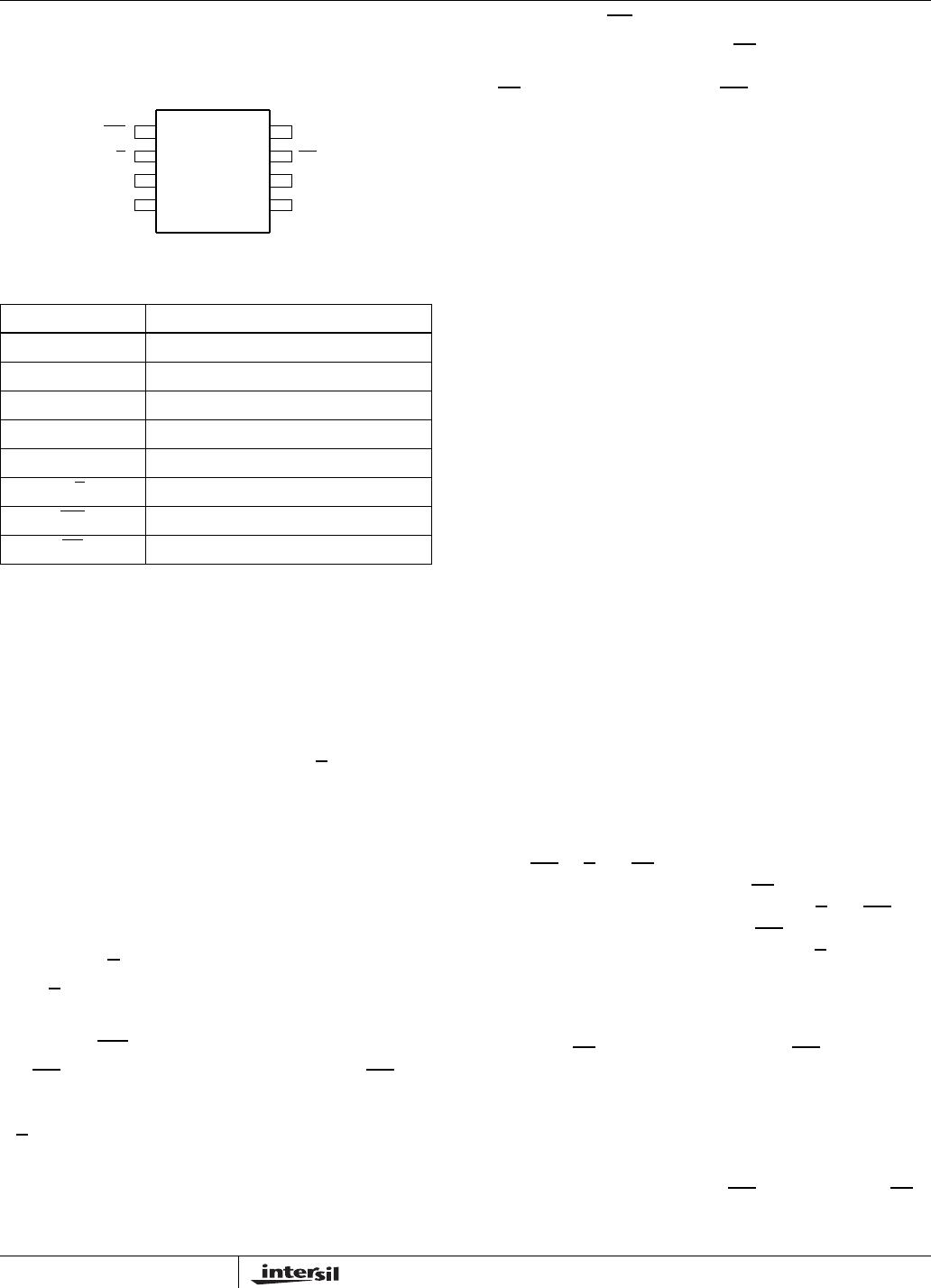
Pin Configuration
X9315
(8 LD MSOP, SOIC, PDIP)
TOP VIEW
Pin Description
R
H
/V
H
and R
L
/V
L
The high (R
H
/V
H
) and low (R
L
/V
L
) terminals of the X9315
are equivalent to the fixed terminals of a mechanical
potentiometer. The minimum voltage is V
SS
and the
maximum is V
CC
. The terminology of R
L
/V
L
and R
H
/V
H
references the relative position of the terminal in relation to
wiper movement direction selected by the U/D
input, and not
the voltage potential on the terminal.
R
W
/V
W
R
W
/V
w
is the wiper terminal and is equivalent to the movable
terminal of a mechanical potentiometer. The position of the
wiper within the array is determined by the control inputs.
The wiper terminal series resistance is typically 200Ω at
V
CC
= 5V.
Up/Down (U/D)
The U/D input controls the direction of the wiper movement
and whether the counter is incremented or decremented.
Increment (INC)
The INC input is negative-edge triggered. Toggling INC will
move the wiper and either increment or decrement the
counter in the direction indicated by the logic level on the
U/D
input.
Chip Select (CS)
The device is selected when the CS input is LOW. The
current counter value is stored in nonvolatile memory when
CS
is returned HIGH while the INC input is also HIGH. After
the store operation is complete the X9315 will be placed in
the low power standby mode until the device is selected
once again.
Principles of Operation
There are three sections of the X9315: the input control,
counter and decode section; the nonvolatile memory; and
the resistor array. The input control section operates just like
an up/down counter. The output of this counter is decoded to
turn on a single electronic switch connecting a point on the
resistor array to the wiper output. Under the proper
conditions the contents of the counter can be stored in
nonvolatile memory and retained for future use. The resistor
array is comprised of 31 individual resistors connected in
series. At either end of the array and between each resistor
is an electronic switch that transfers the connection at that
point to the wiper.
The wiper, when at either fixed terminal, acts like its
mechanical equivalent and does not move beyond the last
position. That is, the counter does not wrap around when
clocked to either extreme.
The electronic switches on the device operate in a “make
before break” mode when the wiper changes tap positions. If
the wiper is moved several positions, multiple taps are
connected to the wiper for t
IW
(INC to V
W
change). The
R
TOTAL
value for the device can temporarily be reduced by
a significant amount if the wiper is moved several positions.
When the device is powered-down, the last wiper position
stored will be maintained in the nonvolatile memory. When
power is restored, the contents of the memory are recalled
and the wiper is set to the value last stored.
Instructions and Programming
The INC, U/D and CS inputs control the movement of the
wiper along the resistor array. With CS
set LOW the device
is selected and enabled to respond to the U/D
and INC
inputs. HIGH to LOW transitions on INC
will increment or
decrement (depending on the state of the U/D
input) a five
bit counter. The output of this counter is decoded to select
one of thirty two wiper positions along the resistive array.
The value of the counter is stored in nonvolatile memory
whenever CS
transitions HIGH while the INC input is also
HIGH.
The system may select the X9315, move the wiper and
deselect the device without having to store the latest wiper
position in nonvolatile memory. After the wiper movement is
performed as described above and once the new position is
reached, the system must keep INC
LOW while taking CS
HIGH. The new wiper position will be maintained until
Pin Names
SYMBOL DESCRIPTION
R
H
/V
H
High terminal
R
W
/V
W
Wiper terminal
R
L
/V
L
Low terminal
V
SS
Ground
V
CC
Supply voltage
U/D
Up/Down control input
INC
Increment control input
CS Chip Select control input
V
CC
CS
INC
U/D
R
H
/V
H
V
SS
1
2
3
4
8
7
6
5
X9315
R
L
/V
L
R
W
/V
W
X9315
5
FN8179.2
December 21, 2009
changed by the system or until a power-up/down cycle
recalled the previously stored data.
This procedure allows the system to always power-up to a
preset value stored in nonvolatile memory; then during
system operation minor adjustments could be made. The
adjustments might be based on user preference, system
parameter changes due to temperature drift, etc...
The state of U/D
may be changed while CS remains LOW.
This allows the host system to enable the device and then
move the wiper up and down until the proper trim is attained.
Power-up and Down Requirements
There are no restrictions on the power-up or power-down
conditions of V
CC
and the voltages applied to the
potentiometer pins provided that V
CC
is always more
positive than or equal to V
H
, V
L
, and V
W
, i.e., V
CC
V
H
, V
L
,
V
W
. The V
CC
ramp rate spec is always in effect.
Mode Selection
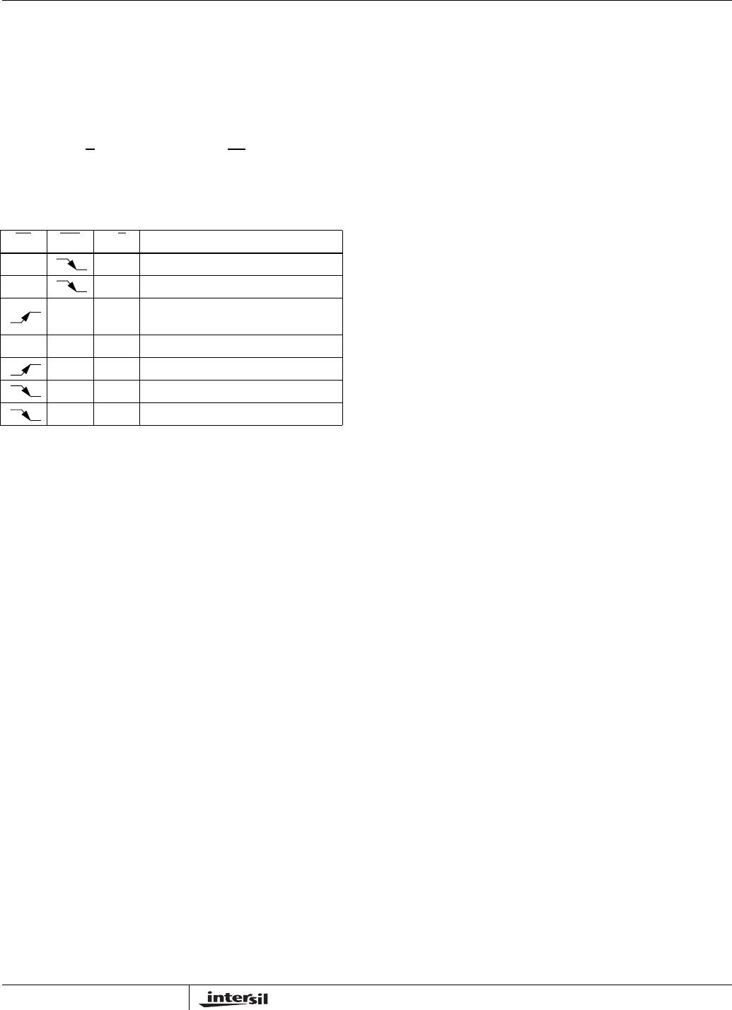
CS INC U/D MODE
L H Wiper up
L L Wiper down
H X Store wiper position to nonvolatile
memory
H X X Standby
L X No store, return to standby
L H Wiper Up (not recommended)
L L Wiper Down (not recommended)
X9315
6
FN8179.2
December 21, 2009
Absolute Maximum Ratings Thermal Information
Temperature under bias. . . . . . . . . . . . . . . . . . . . . .-65°C to +135°C
Storage temperature . . . . . . . . . . . . . . . . . . . . . . . .-65°C to +150°C
Voltage on CS
, INC, U/D, V
H
, V
L
and
V
CC
with respect to V
SS
. . . . . . . . . . . . . . . . . . . . . . . -1V to +7V
ΔV = |V
H
–V
L
| . . . . . . . . . . . . . . . . . . . . . . . . . . . . . . . . . . . . . . . . .5V
I
W
(10 seconds). . . . . . . . . . . . . . . . . . . . . . . . . . . . . . . . . . .±7.5mA
Thermal Resistance (Typical, Notes 3, 4) θ
JA
(°C/W) θ
JC
(°C/W)
8 Ld SOIC . . . . . . . . . . . . . . . . . . . . . . 105 68
8 Ld MSOP. . . . . . . . . . . . . . . . . . . . . . 154 58
8 Ld PDIP. . . . . . . . . . . . . . . . . . . . . . . 85 57
Pb-Free Reflow Profile. . . . . . . . . . . . . . . . . . . . . . . . .see link below
http://www.intersil.com/pbfree/Pb-FreeReflow.asp
Recommended Operating Conditions
Temperature (Commercial) . . . . . . . . . . . . . . . . . . . . . 0°C to +70°C
Temperature (Industrial). . . . . . . . . . . . . . . . . . . . . . .-40°C to +85°C
Supply Voltage (V
CC
) (Note 8) Limits
X9315. . . . . . . . . . . . . . . . . . . . . . . . . . . . . . . . . . . . . . . 5V ± 10%
X9315-2.7. . . . . . . . . . . . . . . . . . . . . . . . . . . . . . . . . . 2.7V to 5.5V
Max Wiper Current, I
W
. . . . . . . . . . . . . . . . . . . . . . . . . . . . .±3.75mA
Max Power Rating . . . . . . . . . . . . . . . . . . . . . . . . . . . . . . . . . .10mW
CAUTION: Do not operate at or near the maximum ratings listed for extended periods of time. Exposure to such conditions may adversely impact product reliability and
result in failures not covered by warranty.
NOTES:
3. θ
JA
is measured with the component mounted on a high effective thermal conductivity test board in free air. See Tech Brief TB379 for details.
4. For θ
JC
, the “case temp” location is taken at the package top center.
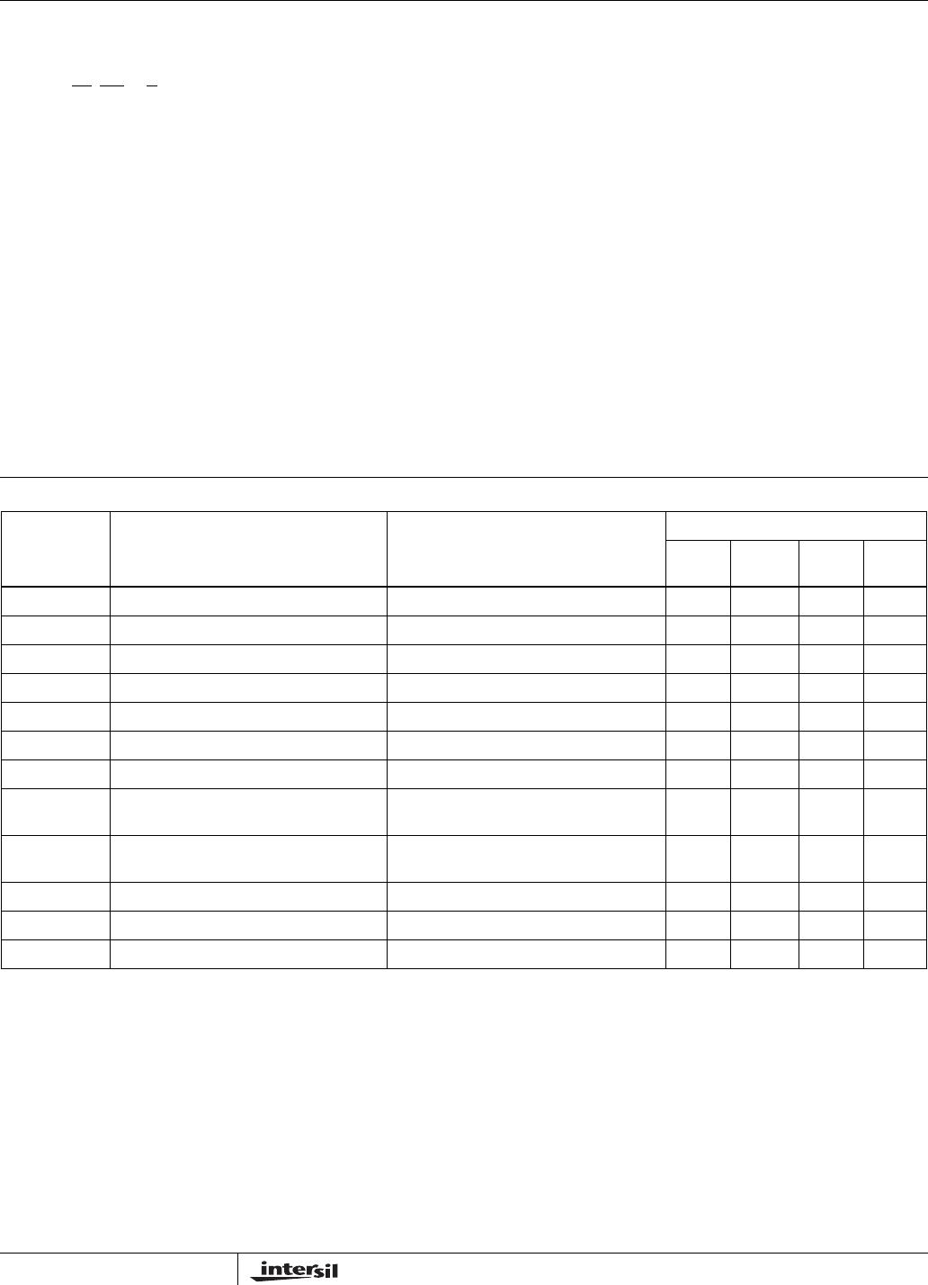
Potentiometer Characteristics (Over recommended operating conditions unless otherwise stated.)
SYMBOL PARAMETER TEST CONDITIONS/NOTES
LIMITS
MIN
(Note 9)
TYP
(Note 8)
MAX
(Note 9) UNIT
End to end resistance tolerance -20 +20 %
V
VH
V
H
terminal voltage 0 V
CC
V
V
VL
V
L
terminal voltage 0 V
CC
V
R
W
Wiper resistance I
W
= [V(R
H
) - V(R
L
)]/ R
TOTAL
, V
CC
= 5V 200 400 Ω
R
W
Wiper resistance I
W
= [V(R
H
) - V(R
L
)]/ R
TOTAL
, V
CC
= 2.7V 400 1000 Ω
Noise Ref: 1kHz -120 dBV
Resolution 3%
Absolute linearity (Note 5) V
w(n)(actual)
- V
w(n)(expected)
±1 MI
(Note 7)
Relative linearity
(Note 6) V
w(n + 1)
- [V
w(n) + MI
0.2MI
(Note 7)
R
TOTAL
temperature coefficient ±300 ppm/°C
Ratiometric temperature coefficient ±20 ppm/°C
C
H
/C
L
/C
W
Potentiometer capacitances See circuit #3 on page 7 10/10/25 pF
NOTES:
5. Absolute linearity is utilized to determine actual wiper voltage versus expected voltage = (V
w(n)
(actual) - V
w(n)
(expected)) = ±1 Ml Maximum.
6. Relative linearity is a measure of the error in step size between taps = R
W(n+1)
- [R
w(n)
+ Ml] = ±0.2 Ml.
7. 1 Ml = Minimum Increment = R
TOT
/31.
8. Typical values are for T
A
= +25°C and nominal supply voltage.
9. Parameters with MIN and/or MAX limits are 100% tested at +25°C, unless otherwise specified. Temperature limits established by
characterization and are not production tested.
X9315

X9315UMZ-2.7

Mfr. #:
Manufacturer:
Renesas / Intersil
Description:
Digital Potentiometer ICs CMOS XDCP 50KOHM 32 TAPS 8LD
Lifecycle:
New from this manufacturer.
Delivery:
DHL FedEx Ups TNT EMS
Payment:
T/T Paypal Visa MoneyGram Western Union