MC100LVEL32DG

MC100LVEL32
www.onsemi.com
4
Table 5. AC CHARACTERISTICS (V
CC
= 3.3 V; V
EE
= 0.0 V or V
CC
= 0.0 V; V
EE
= 3.3 V (Note 1))
Symbol
Characteristic
40°C 25°C 85°C
Unit
Min Typ Max Min Typ Max Min Typ Max
f
max
Maximum Toggle Frequency 2.2 2.5 2.4 2.6 2.6 2.8 GHz
t
PLH
t
PHL
Propagation Delay CLK to Q (Differential)
CLK to Q (Single-Ended)
Reset to Q
350
300
440
500
500
555
530
580
640
370
320
450
510
510
540
550
600
650
410
360
480
540
540
580
590
640
680
ps
t
RR
Reset Recovery 175 50 175 50 175 50 ps
t
PW
Minimum Pulse Width Reset 500 300 500 300 500 300 ps
t
JITTER
Random Clock Jitter (RMS) 2.0 2.0 2.0 ps
V
PP
Input Swing (Differential Swing) (Note 2) 150 1000 150 1000 150 1000 mV
t
r
t
f
Output Rise / Fall Times Q (20%80%) 120 225 320 120 225 320 120 225 320 ps
NOTE: Device will meet the specifications after thermal equilibrium has been established when mounted in a test socket or printed circuit
board with maintained transverse airflow greater than 500 lfpm. Electrical parameters are guaranteed only over the declared
operating temperature range. Functional operation of the device exceeding these conditions is not implied. Device specification limit
values are applied individually under normal operating conditions and not valid simultaneously.
1. V
EE
can vary ±0.3 V.
2. V
PP
(min) is input swing measured single-ended on each input in differential configuration.
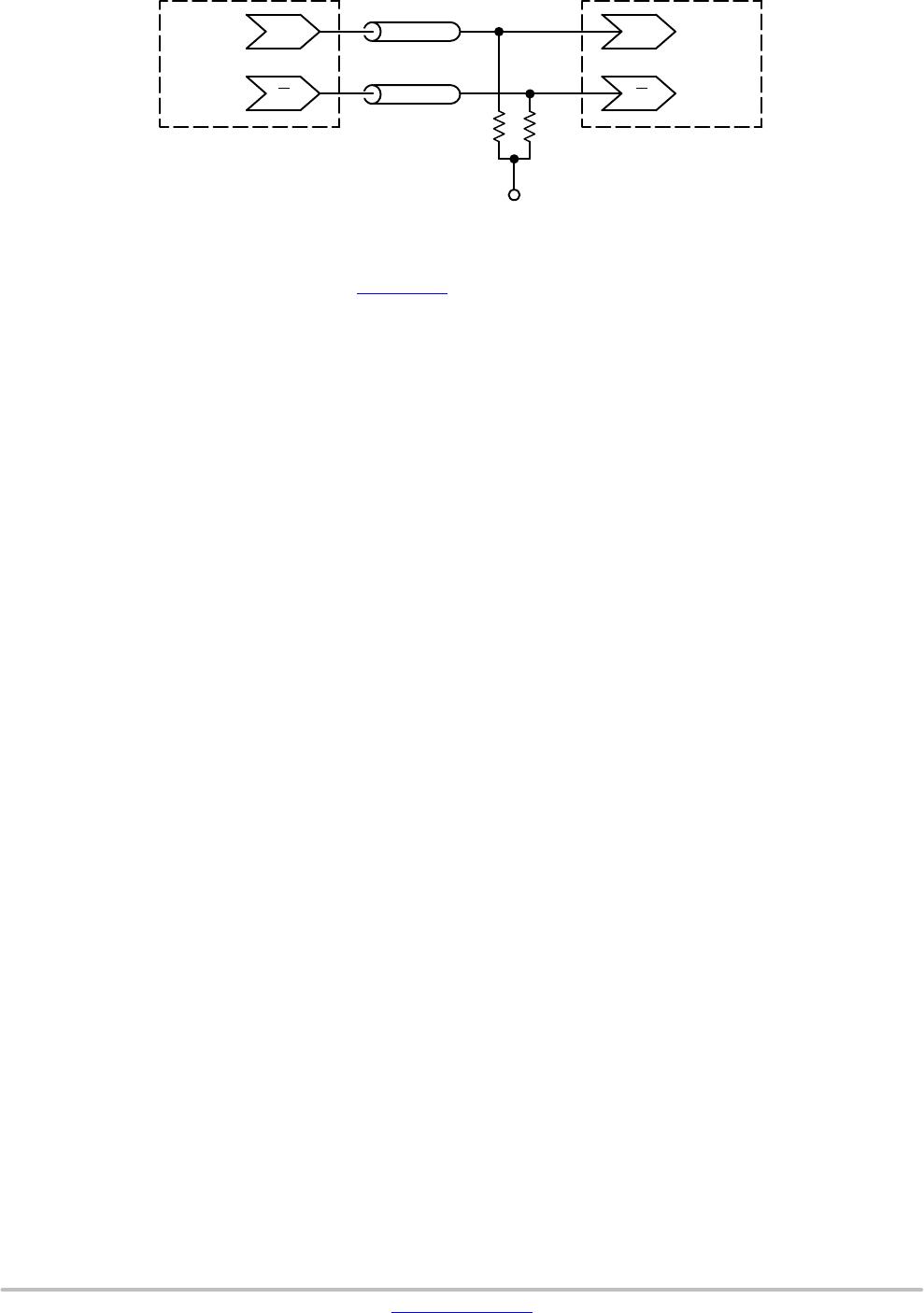
Figure 1. Timing Diagram
CLK
RESET
Q
MC100LVEL32
www.onsemi.com
5
Figure 2. Typical Termination for Output Driver and Device Evaluation
(See Application Note AND8020/D
Termination of ECL Logic Devices)
Driver
Device
Receiver
Device
QD
Q D
Z
o
= 50 W
Z
o
= 50 W
50 W 50 W
V
TT
V
TT
= V
CC
2.0 V
Resource Reference of Application Notes
AN1405/D ECL Clock Distribution Techniques
AN1406/D Designing with PECL (ECL at +5.0 V)
AN1503/D ECLinPS I/O SPiCE Modeling Kit
AN1504/D Metastability and the ECLinPS Family
AN1568/D Interfacing Between LVDS and ECL
AN1672/D The ECL Translator Guide
AND8001/D Odd Number Counters Design
AND8002/D Marking and Date Codes
AND8020/D Termination of ECL Logic Devices
AND8066/D Interfacing with ECLinPS
AND8090/D AC Characteristics of ECL Devices
MC100LVEL32
www.onsemi.com
6
PACKAGE DIMENSIONS
SOIC8 NB
D SUFFIX
CASE 75107
ISSUE AK
SEATING
PLANE
1
4
58
N
J
X 45
_
K
NOTES:
1. DIMENSIONING AND TOLERANCING PER
ANSI Y14.5M, 1982.
2. CONTROLLING DIMENSION: MILLIMETER.
3. DIMENSION A AND B DO NOT INCLUDE
MOLD PROTRUSION.
4. MAXIMUM MOLD PROTRUSION 0.15 (0.006)
PER SIDE.
5. DIMENSION D DOES NOT INCLUDE DAMBAR
PROTRUSION. ALLOWABLE DAMBAR
PROTRUSION SHALL BE 0.127 (0.005) TOTAL
IN EXCESS OF THE D DIMENSION AT
MAXIMUM MATERIAL CONDITION.
6. 75101 THRU 75106 ARE OBSOLETE. NEW
STANDARD IS 75107.
A
B
S
D
H
C
0.10 (0.004)
DIM
A
MIN MAX MIN MAX
INCHES
4.80 5.00 0.189 0.197
MILLIMETERS
B 3.80 4.00 0.150 0.157
C 1.35 1.75 0.053 0.069
D 0.33 0.51 0.013 0.020
G 1.27 BSC 0.050 BSC
H 0.10 0.25 0.004 0.010
J 0.19 0.25 0.007 0.010
K 0.40 1.27 0.016 0.050
M 0 8 0 8
N 0.25 0.50 0.010 0.020
S 5.80 6.20 0.228 0.244
X
Y
G
M
Y
M
0.25 (0.010)
Z
Y
M
0.25 (0.010) Z
S
X
S
M
____
1.52
0.060
7.0
0.275
0.6
0.024
1.270
0.050
4.0
0.155
ǒ
mm
inches
Ǔ
SCALE 6:1
*For additional information on our Pb-Free strategy and soldering
details, please download the ON Semiconductor Soldering and
Mounting Techniques Reference Manual, SOLDERRM/D.
SOLDERING FOOTPRINT*

MC100LVEL32DG

Mfr. #:
Manufacturer:
ON Semiconductor
Description:
Clock Drivers & Distribution 3.3V ECL Divide By 2 Divider
Lifecycle:
New from this manufacturer.
Delivery:
DHL FedEx Ups TNT EMS
Payment:
T/T Paypal Visa MoneyGram Western Union