10
Application Information
Bypassing and PC Board Layout
The HCPL-x710 optocouplers are extremely easy to use. No external interface circuitry is required because the
HCPL-x710 use high-speed CMOS IC technology allowing CMOS logic to be connected directly to the inputs and
outputs.
As shown in Figure 12, the only external components required for proper operation are two bypass capacitors.
Capacitor values should be between 0.01 µF and 0.1 µF. For each capacitor, the total lead length between both
ends of the capacitor and the power-supply pins should not exceed 20 mm. Figure 13 illustrates the recommended
printed circuit board layout for the HPCL-x710.
Figure 12. Recommended Printed Circuit Board layout.
Figure 13. Recommended Printed Circuit Board layout.
Propagation Delay, Pulse-Width Distortion and Propagation Delay Skew
Propagation Delay is a gure of merit that describes how quickly a logic signal propagates through a system. The
propaga tion delay from low to high (t
PLH
) is the amount of time required for an input signal to propagate to the
output, causing the output to change from low to high. Similarly, the propagation delay from high to low (t
PHL
) is
the amount of time required for the input signal to propagate to the output, causing the output to change from
high to low. See Figure 14.
Figure 14.
7
5
6
8
2
3
4
1
GND
2
C1 C2
NC
V
DD2
NC
V
O
V
DD1
V
I
710
YYWW
C1, C2 = 0.01 µF TO 0.1 µF
GND
1
V
DD2
C1 C2
710
YYWW
V
O
GND
2
V
DD1
V
I
GND
1
C1, C2 = 0.01 µF TO 0.1 µF
INPUT
t
PLH
t
PHL
OUTPUT
V
I
V
O
10%
90%90%
10%
V
OH
V
OL
0 V
50%
5 V CMOS
2.5 V CMOS
11
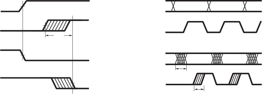
Figure 15. Propagation delay skew waveform Figure 16. Parallel data transmission example
Pulse-width distortion (PWD) is the dierence between
t
PHL
and t
PLH
and often determines the maxi mum data
rate capability of a transmission system. PWD can be
expressed in percent by dividing the PWD (in ns) by
the minimum pulse width (in ns) being trans mitted.
Typically, PWD on the order of 20 - 30% of the minimum
pulse width is tolerable. The PWD specication for the
HCPL-x710 is 8 ns (10%) maximum across recommend-
ed operating condi tions. 10% maximum is dictated
by the most stringent of the three eldbus standards,
PROFIBUS.
Propagation delay skew, t
PSK
, is an important parameter
to con sider in parallel data applications where synchro-
nization of signals on parallel data lines is a concern. If
the parallel data is being sent through a group of op-
tocouplers, dierences in propagation delays will cause
the data to arrive at the outputs of the optocouplers at
dierent times. If this dierence in propagation delay
is large enough it will determine the maximum rate at
which parallel data can be sent through the optocou-
plers.
Propagation delay skew is dened as the dier-
ence between the minimum and maximum propa-
gation delays, either t
PLH
or t
PHL
, for any given group
of optocoup lers that are operating under the same
conditions (i.e., the same drive current, supply volt age,
output load, and operating temperature). As illustrated
in Figure 15, if the inputs of a group of optocouplers
are switched either ON or OFF at the same time, t
PSK
is
the dierence between the shortest propagation delay,
either t
PLH
or t
PHL
, and the longest propagation delay,
either t
PLH
or t
PHL
.
As mentioned earlier, t
PSK
can determine the maximum
parallel data transmission rate. Figure 16 is the timing
diagram of a typical parallel data application with both
the clock and data lines being sent through the opto-
couplers. The gure shows data and clock signals at the
inputs and outputs of the optocouplers. In this case, the
data is assumed to be clocked o of the rising edge of
the clock.
Propagation delay skew repre sents the uncertain-
ty of where an edge might be after being sent
through an optocoupler. Figure 16 shows that there
will be uncertainty in both the data and clock lines.
These two areas of uncertainty must not overlap;
otherwise, the clock signal might arrive before all of
the data outputs have settled, or some of the data
outputs may start to change before the clock signal
has arrived. From these considerations, the absolute
minimum pulse width that can be sent through op-
tocouplers in a parallel application is twice t
PSK
.
A cautious design should use a slightly longer pulse
width to ensure that any additional uncertainty in the
rest of the circuit does not cause a problem.
The HCPL-x710 optocouplers oer the advantage of
guaranteed specications for propagation delays,
pulse-width distortion, and propagation delay skew
over the recommended temperature, and power supply
ranges.
50%
50%
t
PSK
V
I
V
O
V
I
V
O
2.5 V,
CMOS
2.5 V,
CMOS
DATA
INPUTS
CLOCK
DATA
OUTPUTS
CLOCK
t
PSK
t
PSK
12
Optical Isolation for Field Bus Networks
To recognize the full benets of these networks, Avago
optocouplers are recom mended to provide galvanic
isolation. As network communication is bi-direction-
al (involving receiving data from and transmitting
data onto the network), two Avago optocouplers are
needed. By providing galvanic isolation, data integrity is
retained via noise reduction and the elimination of false
signals. In addition, the network receives maximum
protection from power system faults and ground loops.
Within an isolated node, such as the DeviceNet Node
shown in Figure 18, some of the nodes components are
referenced to a ground other than V- of the network.
Figure 17. Typical eld bus communication physical model
These components could include such things as devices
with serial ports, parallel ports, RS-232 and RS-485 type
ports. As shown in Figure 18, power from the network is
used only for the transceiver and input (network) side of
the optocouplers.
Isolation of nodes connected to any of the three types
of digital eld bus networks is best achieved by using
the HCPL-x710 optocouplers. For each network, the
HCPL-x710 satisify the critical propagation delay and
pulse width distortion require ments over the tempera-
ture range of 0 °C to +85 °C, and power supply voltage
range of 4.5 V to 5.5 V.
Digital Field Bus Communication Networks
To date, despite its many draw backs, the 4 - 20 mA
analog current loop has been the most widely accepted
standard for implementing process control systems.
In todays manufacturing environment, however,
automated systems are expected to help manage
the process, not merely monitor it. With the advent
of digital eld bus communication networks such as
DeviceNet, PROFIBUS, and Smart Distributed Systems
(SDS), gone are the days of constrained information.
Controllers can now receive multiple readings from eld
devices (sensors, actuators, etc.) in addition to diagnos-
tic information.
The physical model for each of these digital eld bus
communica tion networks is very similar as shown in
Figure 17. Each includes one or more buses, an interface
unit, optical isolation, transceiver, and sensing and/or
actuating devices.
CONTROLLER
TRANSCEIVER
OPTICAL
ISOLATION
BUS
INTERFACE
TRANSCEIVER
OPTICAL
ISOLATION
BUS
INTERFACE
TRANSCEIVER
OPTICAL
ISOLATION
BUS
INTERFACE
TRANSCEIVER
OPTICAL
ISOLATION
BUS
INTERFACE
TRANSCEIVER
OPTICAL
ISOLATION
BUS
INTERFACE
FIELD BUS
XXXXXX
YYY
SENSOR
DEVICE
CONFIGURATION
MOTOR
STARTER
MOTOR
CONTROLLER

HCPL-0710-000E

Mfr. #:
Manufacturer:
Broadcom / Avago
Description:
High Speed Optocouplers 1Ch 150mA 600mW
Lifecycle:
New from this manufacturer.
Delivery:
DHL FedEx Ups TNT EMS
Payment:
T/T Paypal Visa MoneyGram Western Union